Nanowire circuit architecture

a technology of circuit architecture and wire wires, applied in the field of circuit architecture, to achieve the effect of increasing the clock-frequency of the oscillator and increasing the resolution of the sample-and-hold circui

Inactive Publication Date: 2010-06-24
QUNANO
View PDF11 Cites 32 Cited by
  • Summary
  • Abstract
  • Description
  • Claims
  • Application Information

AI Technical Summary

Benefits of technology

[0017]It is a further advantage of the invention to provide fundamental circuits, including an inverter, a ring-oscillator, a sample-and-hold circuit, and a comparator, based on the nanowire circuit architecture with only two levels of interconnects comprising wrap gate transistors and optionally nanowire resistors and / or nanowire capacitors These are key sub-circuits for the construction of analogue-to-digital converters, but will also find a wider use in other applications. Benefits of the fundamental circuits according to the invention are e.g. increased clock-frequency of the oscillator and increased resolution of the sample-and-hold circuit.

Problems solved by technology

Obviously the prior art has drawbacks with regards to being able to provide fundamental circuits made in a nanowire circuit architecture.

Method used


Image

  • Nanowire circuit architecture
  • Nanowire circuit architecture
  • Nanowire circuit architecture

Examples


Embodiment Construction

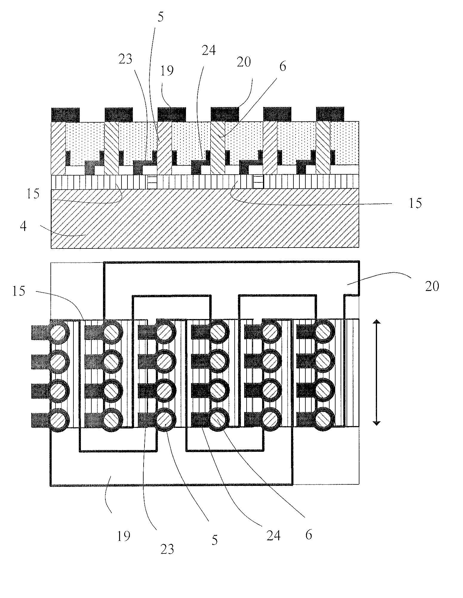
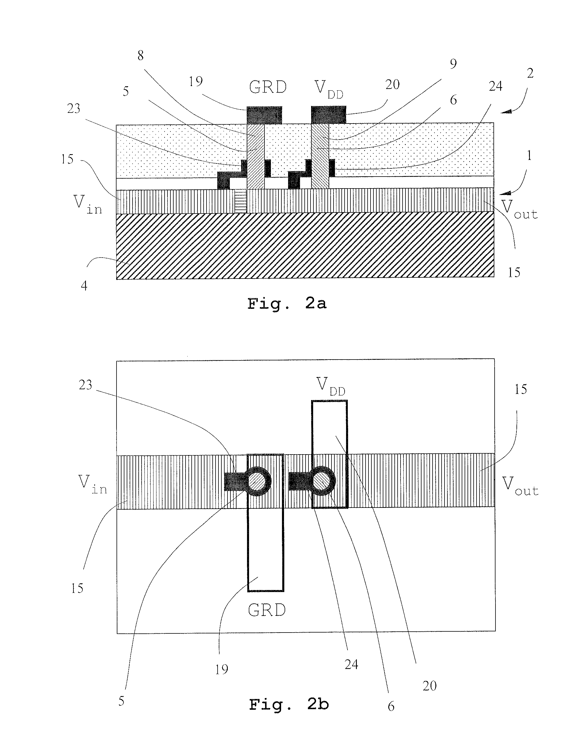
[0025]The present invention is based on nanowires protruding from a substrate, which often is referred to as vertical nanowires. The vertical nanowires may be used as building blocks in nanowire circuits to form e.g. nanowire wrap gate transistors, WIGFETs.

[0026]The nanowires of the present invention may comprise materials selected from the group of Si, Ge, SiGe, III-Vs (such as AlAs, GaAs, InP, GaP, InAs, InSb or alloys thereof), or nitrides (such as GaN, InN, AlN or alloys thereof). However, a person skilled in the art knows that there are more examples of possible materials. The nanowires may further comprise heterostructures distributed along the length thereof and / or radially arranged.

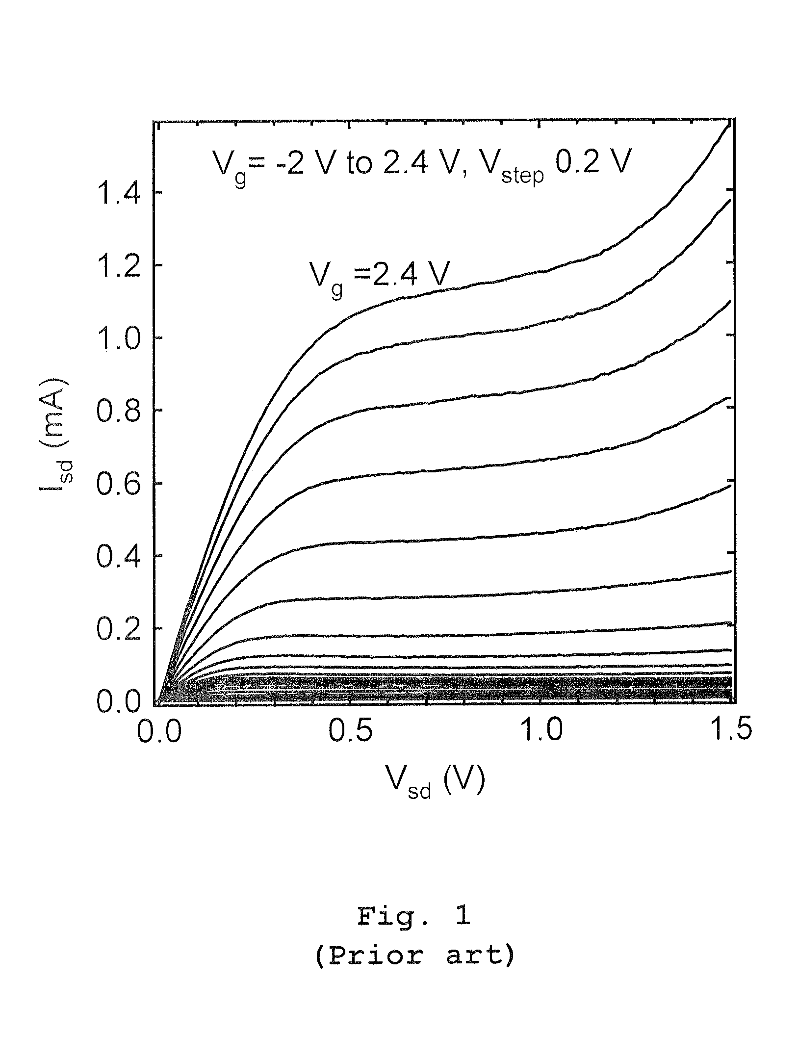
[0027]A nanowire transistor according to the present invention is based on vertical nanowires (typically 1 to 500) in a matrix formation where a metal electrode is wrapped around the nanowires to form the gate electrode. The layout and the processing of such nanowire transistors have previously be...


PUM


Abstract

A nanowire circuit architecture is presented. The technology comprises of nanowire transistors (8,9), and optionally nanowire capacitors (12) and nanowire resistors (11), that are integrated using two levels of interconnects only (1,2). Implementations of ring-oscillators, sample- and-hold circuits, and comparators may be realized in this nanowire circuit architecture. Circuit input and circuit output as well as the transistor connections within each circuit are provided in the two levels of interconnects (1,2).

Description

TECHNICAL FIELD OF THE INVENTION[0001]The present invention relates to a circuit architecture comprising nanowire transistors and optionally nanowire resistors and capacitors. In particular the present invention relates to nanowire transistors having wrap gate electrodes, i.e. so called WIGFETs.BACKGROUND OF THE INVENTION[0002]Power consumption and speed are inherently coupled for a given semiconductor technology. Contact resistances and transport properties are related to the band gap of the semiconductors, which affects current levels and drive voltages. In order to reduce the power consumption and to increase the performance of certain key circuits, for instance for wireless communication, it would be attractive to fabricate those circuits in a different material than Si.[0003]Semiconductor nanowire transistors are considered as one of the candidates in the post-CMOS electronics era. In particular a vertical nanowire configuration allows for a wrap gate formation that efficiently...

Claims


Application Information

Patent Timeline
Patent Type & Authority Applications(United States)
IPC IPC(8): H01L29/66
CPCB82Y10/00H01L21/823487H01L21/823885H01L27/088H01L27/092H01L29/78687H01L29/0676H01L29/78642H01L29/78681H01L29/78684H01L29/0673B82B1/00H01L29/08H03M1/36
Inventor WERNERSSON, LARS-ERIK
Owner QUNANO
Why Eureka
Try Eureka