Vertical channel type nonvolatile memory device and method for fabricating the same

Inactive Publication Date: 2010-06-24
SK HYNIX INC
View PDF4 Cites 302 Cited by
  • Summary
  • Abstract
  • Description
  • Claims
  • Application Information

AI Technical Summary

Problems solved by technology

Volatile memory devices lose data when power is interrupted.
However, planar nonvolatile memory devices fabricated in a single layer over a silicon substrate have limitations in improving integration density due to fine pattern formation as patterning technologies have reached limitations in some aspects.
First, degradation in the layer quality of the tunnel insulation layer 15 causes degradation in da

Method used


Image

  • Vertical channel type nonvolatile memory device and method for fabricating the same
  • Vertical channel type nonvolatile memory device and method for fabricating the same
  • Vertical channel type nonvolatile memory device and method for fabricating the same

Examples


first embodiment

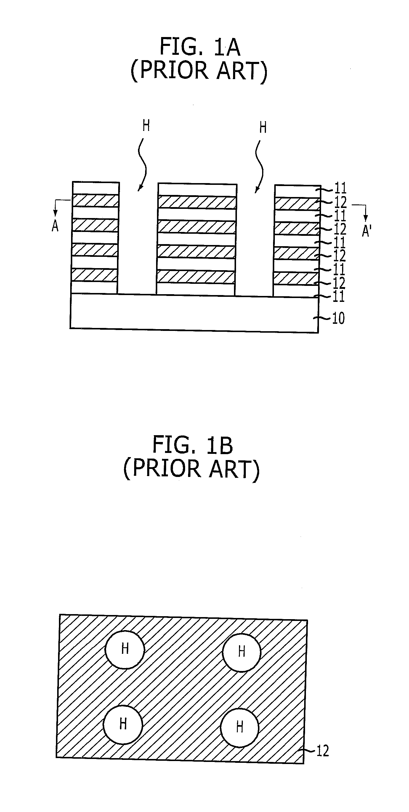
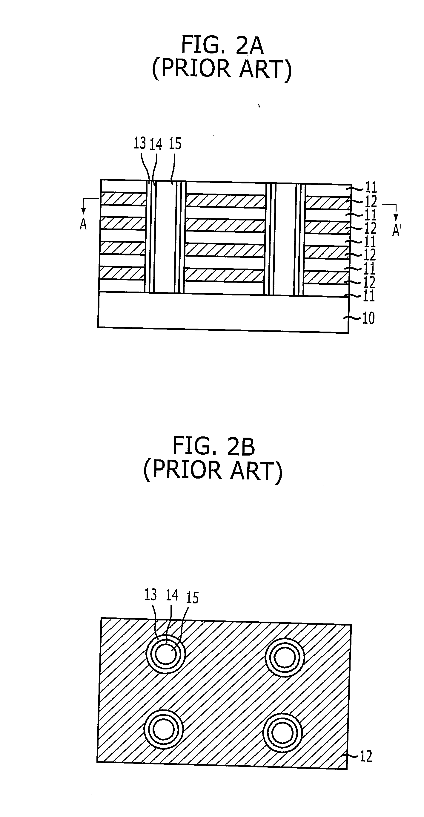
[0047]FIGS. 6A to 11B are diagrams illustrating a method for fabricating a vertical channel type nonvolatile memory device in accordance with the present invention. In particular, a case of using line type openings for removal of sacrificial layers is illustrated. Figures “A” are cross-sectional views illustrating intermediate results, and figures “B” are plan views at height A-A′ of figures “A”.

[0048]Referring to FIGS. 6A and 6B, a plurality of interlayer dielectric layers 21 and a plurality of sacrificial layers 22 are alternately formed on a substrate 20 where a lower structure including a source line, a lower selection transistor, and the like is formed.

[0049]The source line may include a silicon substrate, a conductive material layer, a material layer formed by doping impurities into an insulator, or a metal layer. The interlayer insulation layer 21 separates a plurality of memory cells from one another, where the plurality of memory cells constitutes a string, and may be forme...

second embodiment

[0117]A method for forming a gate electrode in accordance with the present invention will be described hereinafter.

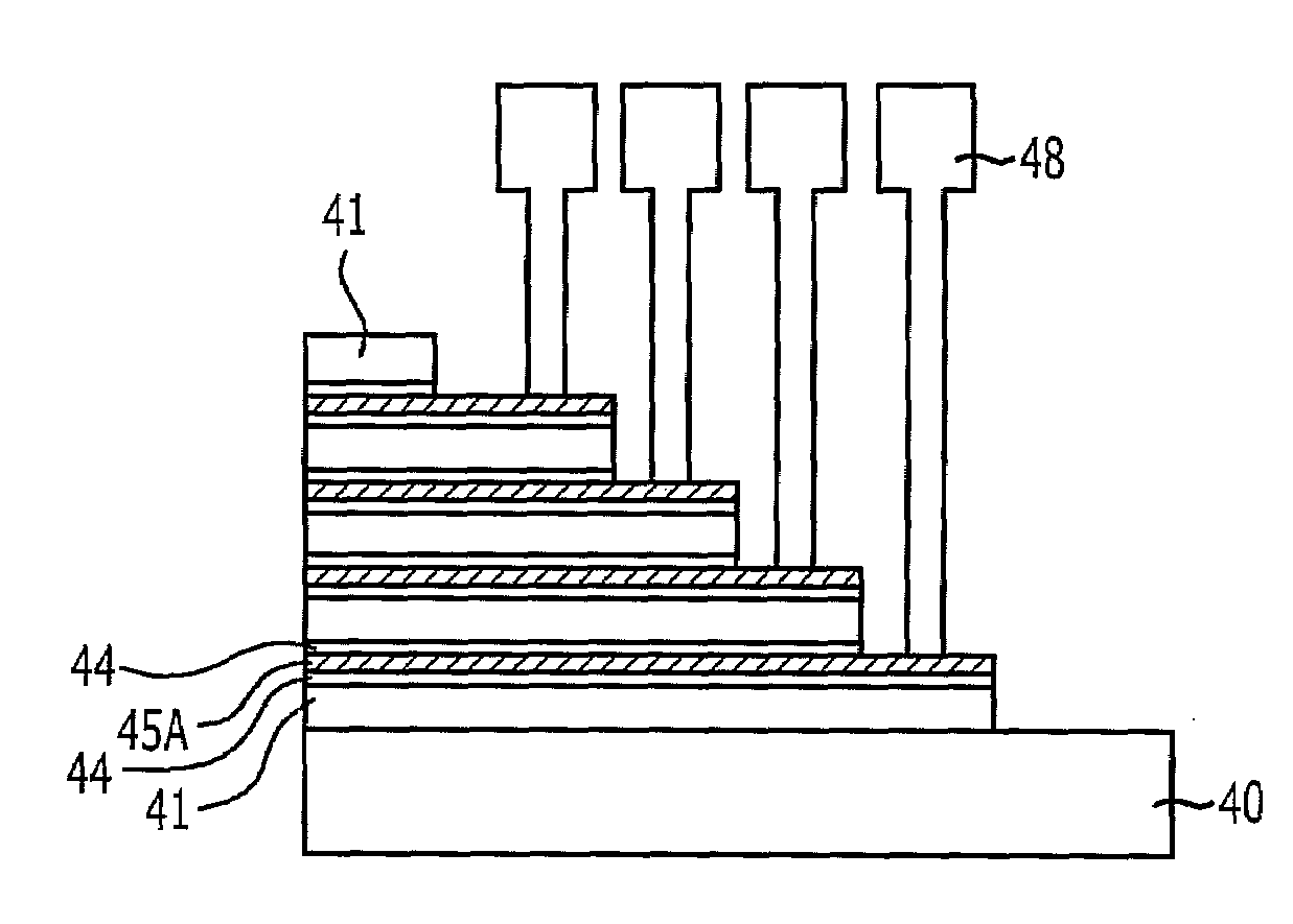
[0118]Referring to FIGS. 25A and 25B, conductive layers 45 for gate electrode are formed over a resulting structure where the tunnel insulation layer, the charge trap layer, the charge blocking layer 44 are formed, so that the opened region between the multi-layered interlayer dielectric layers are filled. At this point, the openings T3″ for removal of the sacrificial layer are completely filled with the conductive layers 45 for gate electrode.

[0119]Referring to FIGS. 26A and 26B, the conductive layers 45 for gate electrode are selectively etched to separate gate electrodes 45A of the memory cells from one another, the memory cells being stacked along the channels 43.

[0120]The conductive layers 45 for gate electrode may be etched by a blanket etch process. When the blanket etch process is performed, the tunnel insulation layer, the charge trap layer, and the charge bloc...


PUM


Abstract

A method for fabricating, a vertical channel type nonvolatile memory device includes: alternately forming a plurality of sacrificial layers and a plurality of interlayer dielectric layers over a semiconductor substrate; etching the sacrificial layers and the interlayer dielectric layers to form a plurality of first openings for channel each of which exposes the substrate; filling the first openings to form a plurality of channels protruding from the semiconductor substrate; etching the sacrificial layers and the interlayer dielectric layers to form second openings for removal of the sacrificial layers between the channels; exposing sidewalls of the channels by removing the sacrificial layers exposed by the second openings; and forming a tunnel insulation layer, a charge trap layer, a charge blocking layer, and a conductive layer for gate electrode on the exposed sidewalls of the channels.

Description

CROSS-REFERENCES TO RELATED APPLICATIONS[0001]The present application claims priority of Korean Patent Application Nos. 10-2008-0133015 and 10-2009-0031902, filed on Dec. 24, 2008, and Apr. 13, 2009, respectively, the disclosure of each of which is incorporated herein by reference in their entirety.BACKGROUND OF THE INVENTION[0002]The present invention relates to a nonvolatile memory device and a method for fabricating the same, and more particularly, to a vertical channel type nonvolatile memory device and a method for fabricating the same.[0003]Memory devices are classified into volatile memory devices and nonvolatile memory devices according to whether data is retained when power is interrupted. Volatile memory devices lose data when power is interrupted. Examples of volatile memory devices include dynamic random access memory (DRAM) and static random access memory (SRAM). In contrast, nonvolatile memory devices retain stored data even when power is interrupted. Examples of nonvo...

Claims


Application Information

Patent Timeline
IPC IPC(8): H01L29/792H01L21/28
CPCH01L27/11578H01L27/11582H01L27/088H01L29/7926H01L29/792H10B43/20H10B43/27
Inventor CHO, HEUNG-JAEKIM, YONG-SOOKIM, BEOM-YONGCHOI, WON-JOONAHN, JUNG-RYUL
Owner SK HYNIX INC
Why Eureka
Try Eureka