Compact Device Housing and Assembly Techniques Therefor

a technology of electronic devices and housings, applied in the direction of electrical apparatus casings/cabinets/drawers, coupling device connections, instruments, etc., can solve the problems of increasing the difficulty of assembly and repair, tedious and difficult assembly and repair of electronic devices, etc., to facilitate the formation of compact electronic devices and/or their assembly, facilitate not only assembly but also repair, and improve cosmetics

Inactive Publication Date: 2010-06-24
APPLE INC
View PDF100 Cites 34 Cited by
  • Summary
  • Abstract
  • Description
  • Claims
  • Application Information

AI Technical Summary

Benefits of technology

[0009]One aspect of the invention pertains to substrate arrangements for use in electronic device assemblies. The substrate arrangements can include multiple-part substrates that are able to be interconnected and utilized in confined spaces. A multiple-part substrate can pertain to a plurality of printed circuit boards that are electrically connected together when assembled into a printed circuit board arrangement. In one implementation, the printed circuit boards can be arranged around an electrical component (e.g., peripheral bus connector). The use of multiple printed circuit boards that are physically configured around other electrical components facilitates formation of compact electronic devices and/or their assembly.
[0010]Another aspect of the invention pertains to a clip for use in electronic device assemblies. The clip provides mechanical and electrical interconnection between two electrical structures, such as a contact pin and an elect

Problems solved by technology

There highly portable electronic devices are typically provided in small housings which makes both assembly and repair tedi

Method used


Image

  • Compact Device Housing and Assembly Techniques Therefor
  • Compact Device Housing and Assembly Techniques Therefor
  • Compact Device Housing and Assembly Techniques Therefor

Examples


Embodiment Construction

[0029]The invention pertains to compact electronic devices that have high density electronic device assemblies and / or to techniques for forming high density electronic device assemblies.

[0030]Embodiments of the invention are discussed below with reference to FIGS. 1-8B. However, those skilled in the art will readily appreciate that the detailed description given herein with respect to these figures is for explanatory purposes as the invention extends beyond these limited embodiments.

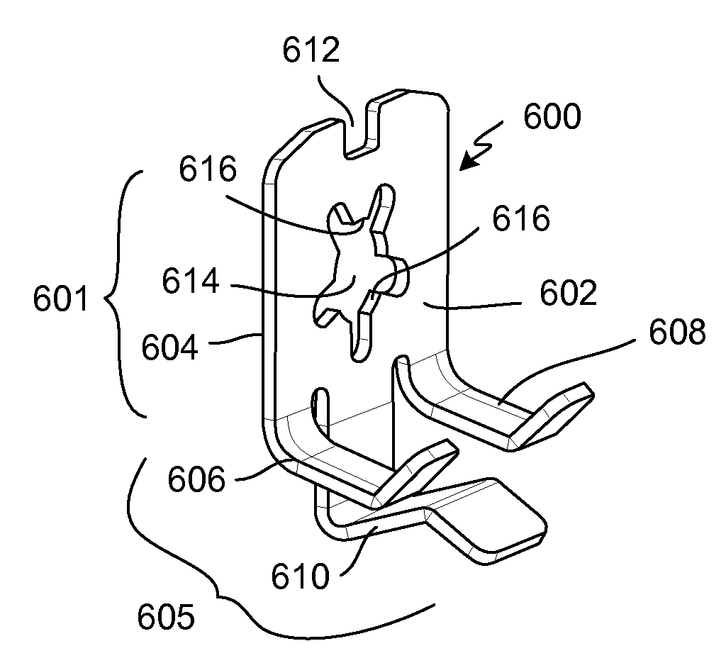
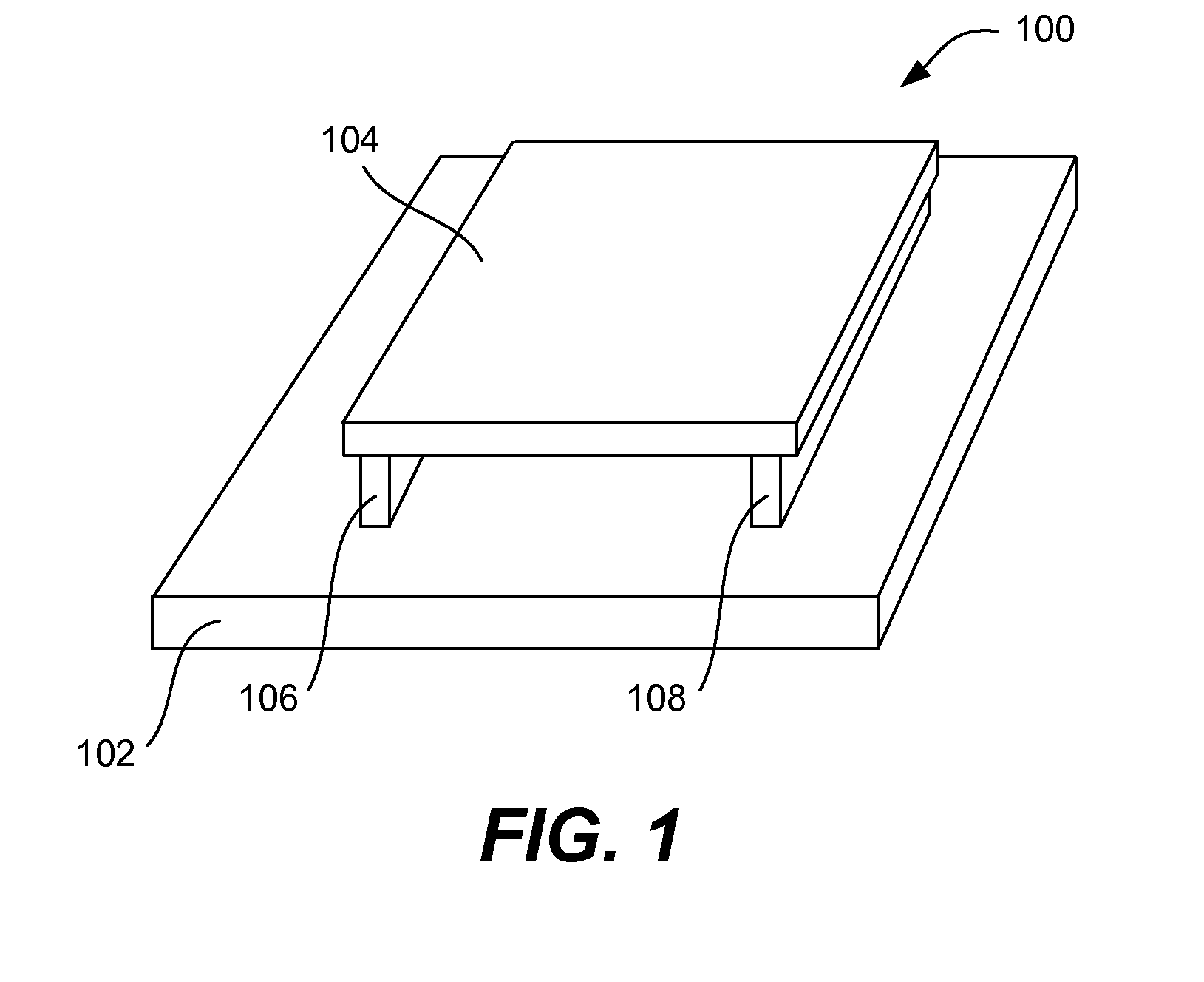
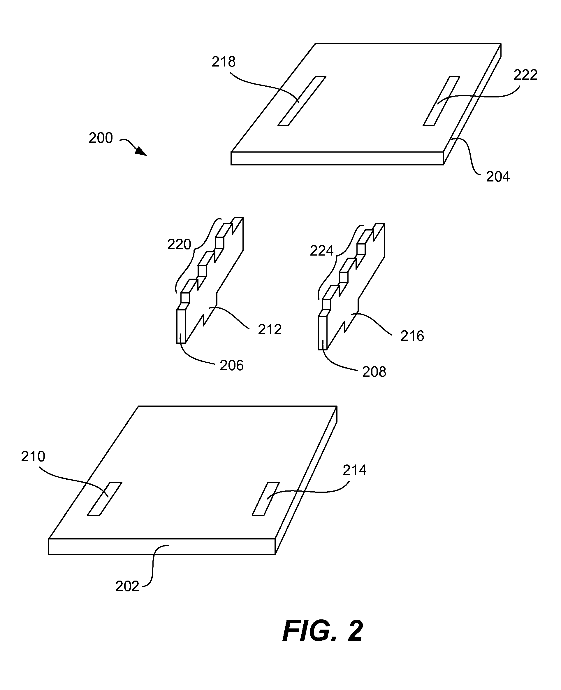
[0031]One aspect of the invention pertains to substrate arrangements for use in electronic device assemblies. The substrate arrangements can include multiple-part substrates that are able to be interconnected and utilized in confined spaces. A multiple-part substrate can pertain to a plurality of printed circuit boards that are electrically connected together when assembled into a printed circuit board arrangement. In one implementation, the printed circuit boards can be arranged around an electrical com...


PUM

PropertyMeasurementUnit
Timeaaaaaaaaaa
Densityaaaaaaaaaa
Mechanical propertiesaaaaaaaaaa

Abstract

High density electronic device assemblies and techniques for forming high density electronic device assemblies are disclosed. These assemblies and techniques can be used to form compact electronic devices. In one embodiment, substrate arrangements that include a multiple-part substrate can be used to form a high density electronic device assembly. In another embodiment, one or more clips can be used in a high density electronic device assembly to provide mechanical and electrical interconnection between electrical structures that are to be removably coupled together as parts of the high density electronic device assembly. In still another embodiment, a removable cap (and a method for forming the removable cap) can be used for an electronic device housing.

Description

CROSS-REFERENCE TO RELATED APPLICATION[0001]This application claims priority to U.S. Provisional Patent Application No. 61 / 140,599, filed Dec. 23, 2008, entitled “COMPACT DEVICE HOUSING AND ASSEMBLY TECHNIQUES THEREFOR”, which is hereby incorporated herein by reference.BACKGROUND OF THE INVENTION[0002]1. Field of the Invention[0003]The present invention relates to electronic device assemblies and, more particularly, to high density electronic device assemblies.[0004]2. Description of the Related Art[0005]Today, many electronic devices are highly portable so that they can be easily transported by their users. There are many examples of highly portable electronic devices, such as mobile phones, portable media players, personal digital assistants, portable power adapter, etc. There highly portable electronic devices are typically provided in small housings which makes both assembly and repair tedious and difficult.[0006]Given the desire to make electronic devices smaller, there is a ne...

Claims


Application Information

Patent Timeline
IPC IPC(8): H01R4/48H05K1/11H05K5/00H01S4/00H05K7/00
CPCH01R9/091H01R12/57H01R13/111H01R13/6675H05K1/141Y10T29/49002H05K3/366H05K2201/048H05K2201/09181H05K2201/10189Y10T29/49117H05K1/145H01R12/58H01R12/00
Inventor LIN, WEY-JIUNPAN, KEVINDE LA CRUZ, CONRADO SACLUTI
Owner APPLE INC
Why Eureka
Try Eureka