Thermoelectric device and fabrication method thereof, chip stack structure, and chip package structure

a fabrication method and thermoelectric device technology, applied in the direction of thermoelectric device manufacture/treatment, semiconductor devices, semiconductor device details, etc., can solve the problems of increasing the thickness of difficult to integrate the thermoelectric device and increasing the thickness of the bonding wire. , to achieve the effect of reducing the volume of the thermoelectric device and being easy to integrate into the chip package structure or the chip stack structur

Inactive Publication Date: 2010-07-01
IND TECH RES INST
View PDF13 Cites 55 Cited by
  • Summary
  • Abstract
  • Description
  • Claims
  • Application Information

AI Technical Summary

Benefits of technology

[0008]Accordingly, the disclosure is directed to a thermoelectric device which can be easily integrated into a chip package structure or a chip stack structure.
[0011]The disclosure is directed to a fabrication method of a thermoelectric device, wherein the thermoelectric device can be easily integrated into a chip package structure or a chip stack structure.
[0016]As described above, in the disclosure, a thermoelectric device is coupled to an external power source through conductive vias. Thus, the thermoelectric device in the disclosure does not need to be coupled to the external power source through any power line or bonding wire (as in the conventional technique). Accordingly, in the disclosure the volume of the thermoelectric device is reduced and the thermoelectric device can be easily integrated into a chip package structure or a chip stack structure.

Problems solved by technology

However, because the power lines will interfere with a sealed structure, it is difficult to integrate the thermoelectric device into a chip package structure.
However, these metal pads take up the limited surface of the carrier, and the bonding wires increase the thickness of the chip package structure.

Method used


Image

  • Thermoelectric device and fabrication method thereof, chip stack structure, and chip package structure
  • Thermoelectric device and fabrication method thereof, chip stack structure, and chip package structure
  • Thermoelectric device and fabrication method thereof, chip stack structure, and chip package structure

Examples


Embodiment Construction

[0026]Reference will now be made in detail to the present preferred embodiments of the disclosure, examples of which are illustrated in the accompanying drawings. Wherever possible, the same reference numbers are used in the drawings and the description to refer to the same or like parts.

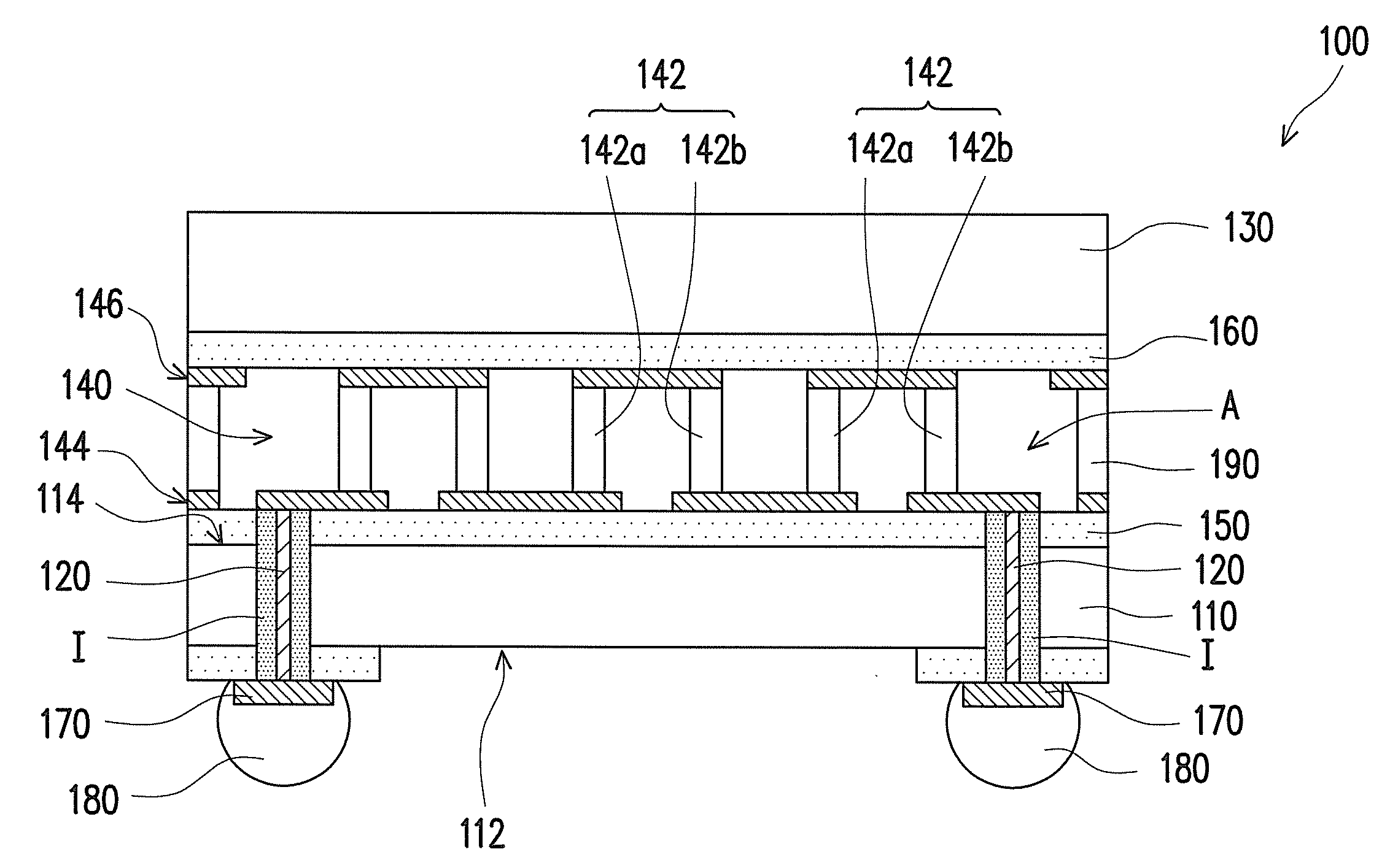
[0027]FIG. 1 is a cross-sectional view of a thermoelectric device according to an embodiment of the disclosure. Referring to FIG. 1, in the present embodiment, the thermoelectric device 100 includes a first substrate 110, a plurality of conductive vias 120, a second substrate 130, a thermoelectric couple module 140, a first insulation layer 150, and a second insulation layer 160.

[0028]In the present embodiment, the first substrate 110 may be a metal substrate, a silicon substrate, or other suitable substrate, wherein the silicon substrate may be a chip. The first substrate 110 has a first surface 112 and a second surface 114 opposite to the first surface 112. The conductive vias 120 run through the ...


PUM


Abstract

A thermoelectric device including a first substrate, a plurality of conductive vias, a second substrate, a thermoelectric couple module, a first insulation layer, and a second insulation layer is provided. The first substrate has a first surface and a second surface opposite to each other. The conductive vias running through the first substrate respectively connect the first and the second surface. The second substrate faces the second surface of the first substrate. The thermoelectric couple module including a plurality of thermoelectric couples connected with each other in series is disposed between the first and the second substrate and coupled to the conductive vias. The first insulation layer is disposed between the thermoelectric couple module and the first substrate. The second insulation layer is disposed between the thermoelectric couple module and the second substrate.

Description

CROSS-REFERENCE TO RELATED APPLICATION[0001]This application claims the priority benefit of Taiwan application serial no. 97151887, filed on Dec. 31, 2008. The entirety of the above-mentioned patent application is hereby incorporated by reference herein and made a part of specification.BACKGROUND[0002]1. Technical Field[0003]The disclosure generally relates to a heat dissipation device and a fabrication method thereof and a chip package structure and a chip stack structure having the heat dissipation device, and more particularly, to a thermoelectric device and a fabrication method thereof and a chip package structure and a chip stack structure having the thermoelectric device.[0004]2. Description of Related Art[0005]Thermoelectric devices made of thermoelectric semiconductor materials are broadly applied to cooling or heating apparatuses because they do not need any liquid or gas as coolant and have such advantages as non-stop operation, contamination-free, moving-part-free, noise-...

Claims


Application Information

Patent Timeline
Patent Type & Authority Applications(United States)
IPC IPC(8): H01L35/28H01L21/50H01L35/34
CPCH01L23/3675H01L23/38H01L23/481H01L24/13H01L24/16H01L24/17H01L24/81H01L25/0657H01L35/32H01L2224/0401H01L2224/0603H01L2224/13023H01L2224/13099H01L2224/1403H01L2224/48091H01L2224/48227H01L2224/73253H01L2224/81193H01L2224/81194H01L2224/81801H01L2225/0651H01L2225/06513H01L2225/06517H01L2225/06589H01L2924/1532H01L2924/00014H01L24/48H01L2924/00013H01L2924/01033H01L2224/06102H01L2924/181H01L2924/00H01L2924/1815H01L2224/45099H01L2224/45015H01L2924/207H01L2224/16105H01L2224/1411H10N10/17
Inventor LIU, CHUN-KAICHANG, SHU-MING
Owner IND TECH RES INST
Why Eureka
Try Eureka