Substrate structure and manufacturing method thereof

a technology of substrate structure and manufacturing method, which is applied in the manufacture of resistive materials, cable/conductor materials, metallic pattern materials, etc., can solve the problem of shifting problem of conductive parts, and achieve the effect of improving the quality of electrical connection of conductive parts

Active Publication Date: 2010-07-01
ADVANCED SEMICON ENG INC
View PDF9 Cites 6 Cited by
  • Summary
  • Abstract
  • Description
  • Claims
  • Application Information

AI Technical Summary

Benefits of technology

[0009]The invention is directed to a substrate structure and a manufacturing method thereof. The conductive part of the substrate structure completely fills the corner of the hole, so that the quality of electrical connection of the conductive part is improved.

Problems solved by technology

Thus, the formation of the conductive part in subsequent process will be affected so that shift problem will occur to the conductive part as well.

Method used


Image

  • Substrate structure and manufacturing method thereof
  • Substrate structure and manufacturing method thereof
  • Substrate structure and manufacturing method thereof

Examples


Embodiment Construction

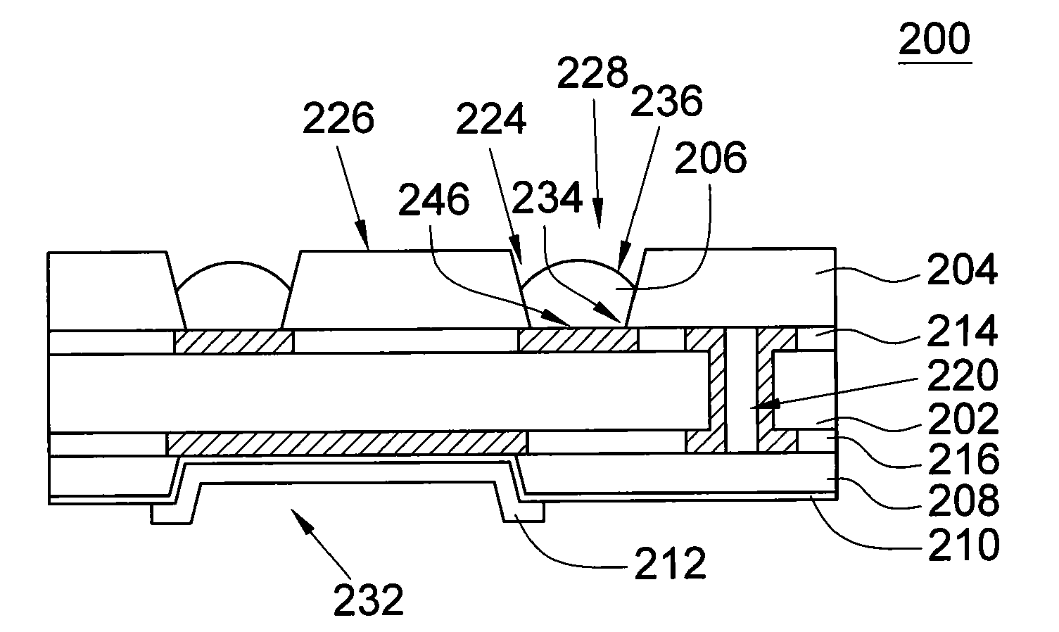
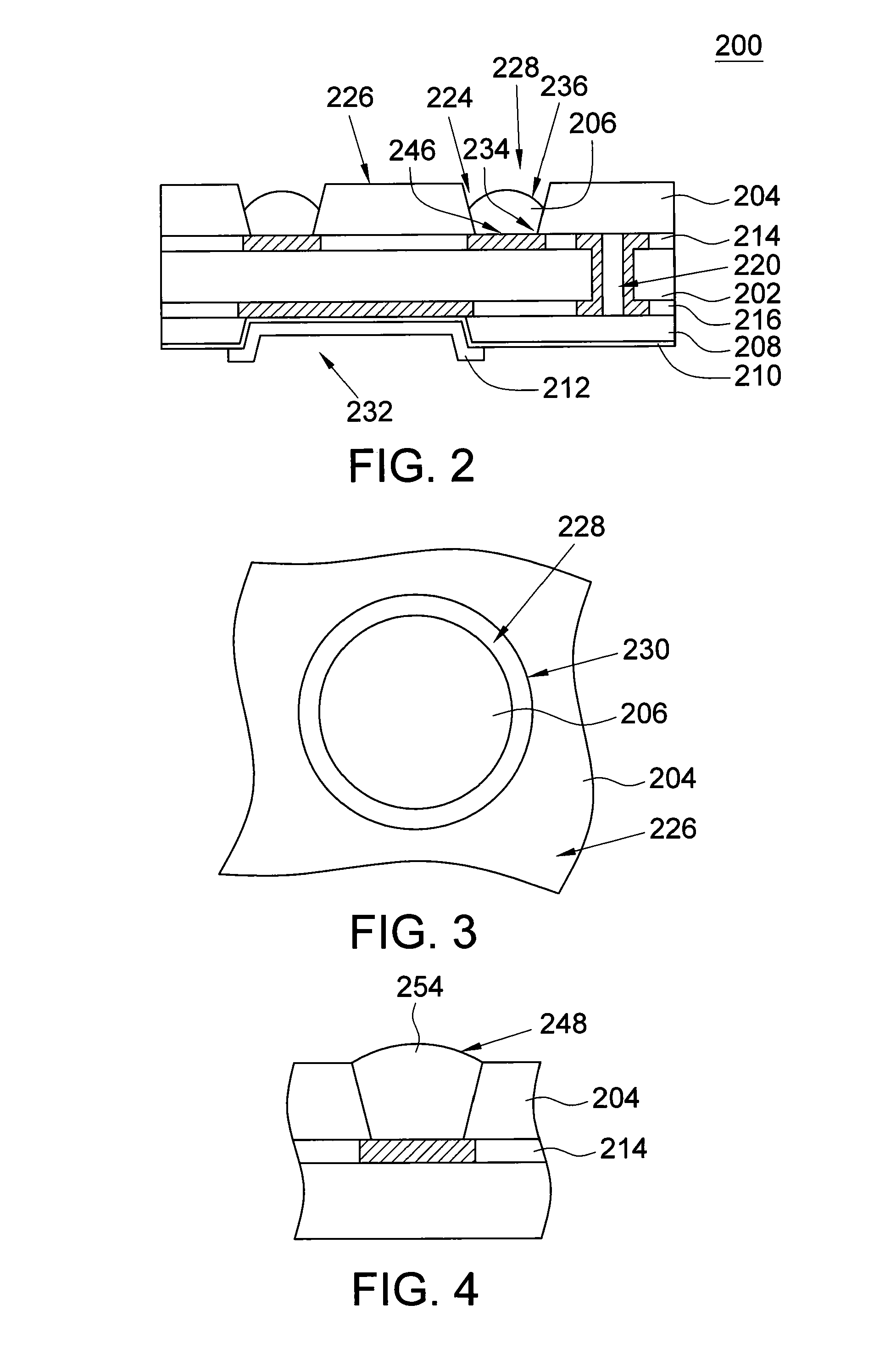
[0028]Referring to FIG. 2, a substrate structure according to a preferred embodiment of the invention is shown. The present embodiment of the invention is exemplified by a substrate structure 100 applicable to flip chip. The substrate structure 200 includes a substrate 202, a first insulation layer 204, a conductive part 206, a second insulation layer 208, a first seed layer 210 and a conductive layer 212.

[0029]The substrate 202 has a first circuit pattern layer 214 and a second circuit pattern layer 216, which are located on two opposite surfaces of the substrate 202. The substrate 202 further has a via hole 220 through which the first circuit pattern layer 214 and the second circuit pattern layer 216 are electrically connected. Besides, the first insulation layer 204, such as a solder mask, is formed on the first circuit pattern layer 214. The first insulation layer 204 has a first insulation hole 224 which exposes a first opening 228 on the outer surface 226 of the first insulati...


PUM

PropertyMeasurementUnit
conductiveaaaaaaaaaa
coefficient of thermal expansionaaaaaaaaaa
surface tensionaaaaaaaaaa

Abstract

A substrate structure is provided. The substrate structure includes a substrate, a first insulation layer, a conductive part, a second insulation layer, a seed layer and a conductive layer. The substrate has a first circuit pattern layer and a second circuit pattern layer, which are located on two opposite surfaces of the substrate respectively. The first insulation layer formed on the first circuit pattern layer has a first insulation hole, which exposes a first opening in the outer surface of the first insulation layer. The conductive part formed on the first insulation hole for electrically connecting with a chip is enclosed by the edge of the first opening. The second insulation layer formed on the second circuit pattern layer has a second insulation hole in which the seed layer is formed. The conductive layer is formed on the seed layer for electrically connecting with a circuit board.

Description

[0001]This application claims the benefit of Taiwan application Serial No. 97151291, filed Dec. 29, 2008, the subject matter of which is incorporated herein by reference.BACKGROUND OF THE INVENTION[0002]1. Field of the Invention[0003]The invention relates in general to a substrate structure and a manufacturing method thereof, and more particularly to a substrate structure applicable to a flip chip and a manufacturing method thereof.[0004]2. Description of the Related Art[0005]Referring to FIG. 1A, a generally known substrate structure is shown. The generally known substrate structure, such as the substrate structure 100 applicable to flip chip, has a substrate 116, a conductive part 102 and an insulation layer 104. The conductive part 102 is for electrically connecting with a chip (not illustrated) such as a flip chip. A part of the conductive part 102 contacts the insulation layer 104 such as a solder mask. The dry film 106 of FIG. 1A is for defining the range of the conductive par...

Claims


Application Information

Patent Timeline
Patent Type & Authority Applications(United States)
IPC IPC(8): H05K1/09H05K1/00B44C1/22
CPCH01L21/4846H01L23/49811H01L23/49816H01L23/49822H01L23/49827H05K1/112H05K3/243H05K3/4007H05K3/42H05K2201/0352H05K2201/0367H05K2201/09436H05K2201/09509H05K2201/10674H05K2203/054H05K2203/072H05K2203/0723H05K2203/1572H01L2924/0002H01L2924/00
Inventor LEE, CHIH-CHENG
Owner ADVANCED SEMICON ENG INC
Why Eureka
Try Eureka