Capacitive touch sensing assembly

a touch sensor and capacitive technology, applied in the field of capacitive touch sensing assembly, can solve the problems of deformation and distortion of image displayed from the touch panel, the sensitivity and precision of the capacitive touch sensing signal will be damaged, and the panel will not sustain stress and then deformed and damaged, so as to reduce the cost and simplify the process.

Active Publication Date: 2010-07-01
YOUNG FAST OPTOELECTRONICS
View PDF8 Cites 27 Cited by
  • Summary
  • Abstract
  • Description
  • Claims
  • Application Information

AI Technical Summary

Benefits of technology

[0003]Accordingly, the primary object of the present invention is to provide a touch sensing assembly with the X and Y axis traces in the same plane so as the traces can be formed more precisely for the sensitivity and the precision of a sensing effect. Also, the process is simplified and the cost is lowered by reducing layers of the thinned plate body.
[0004]A secondary object of the present invention is to provide a touch sensing assembly with the X and Y axis traces in the same plane so that the un-patterned area ratio is substantially reduced. The assembly will be uniformly pervious to light and the image distortion of the screen under the touch panel will be corrected.

Problems solved by technology

The panel will not repeatedly sustain stress and then deformed and damaged because an input is performed without strongly pressing on the panel.
When assembling the X and Y sensing traces of the two different layers, a misalignment is happened and the sensitivity and precision of the sensing signal of the capacity will be damaged.
However, the traces and the un-patterned area on different layers are differently pervious to light, the light passing through the panel will be refracted and causes a deformation and distortion of image displayed from the screen under the touch panel.

Method used


Image

  • Capacitive touch sensing assembly
  • Capacitive touch sensing assembly
  • Capacitive touch sensing assembly

Examples


Embodiment Construction

[0011]In order that those skilled in the art can further understand the present invention, a description will be provided in the following in details. However, these descriptions and the appended drawings are only used to cause those skilled in the art to understand the objects, features, and characteristics of the present invention, but not to be used to confine the scope and spirit of the present invention defined in the appended claims.

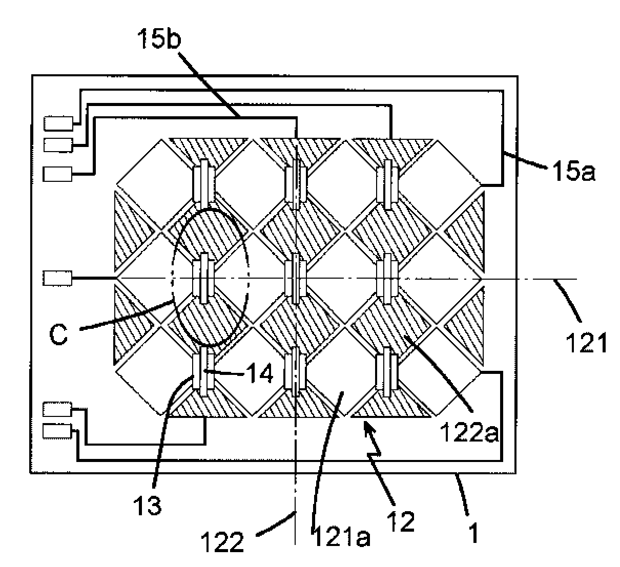
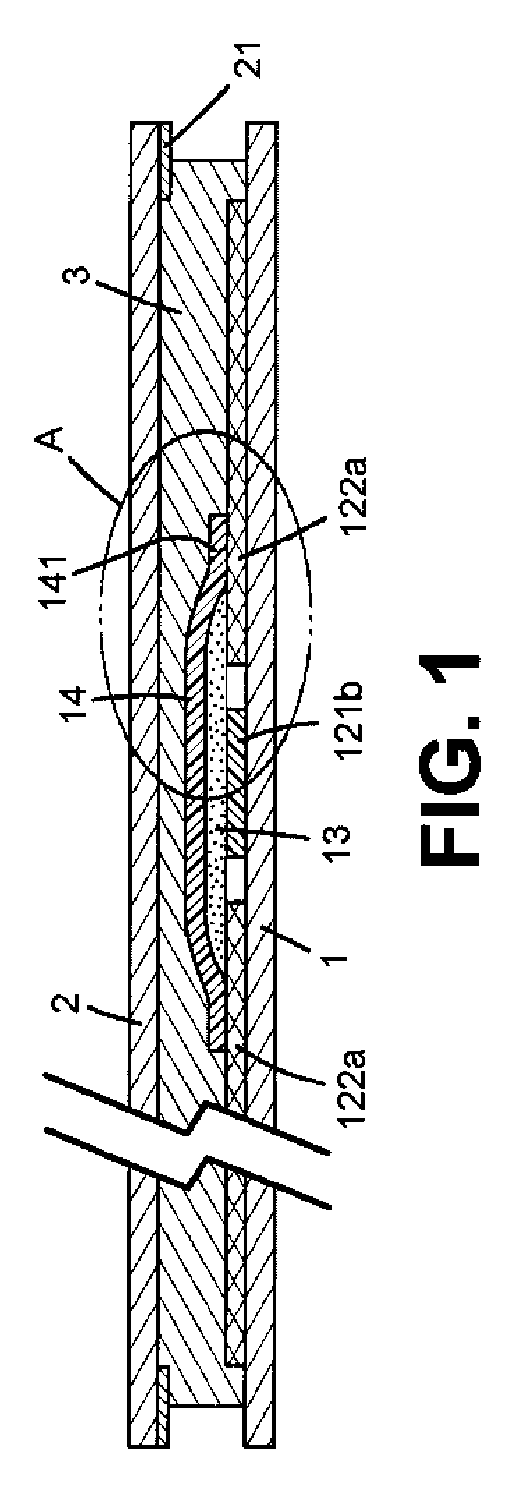
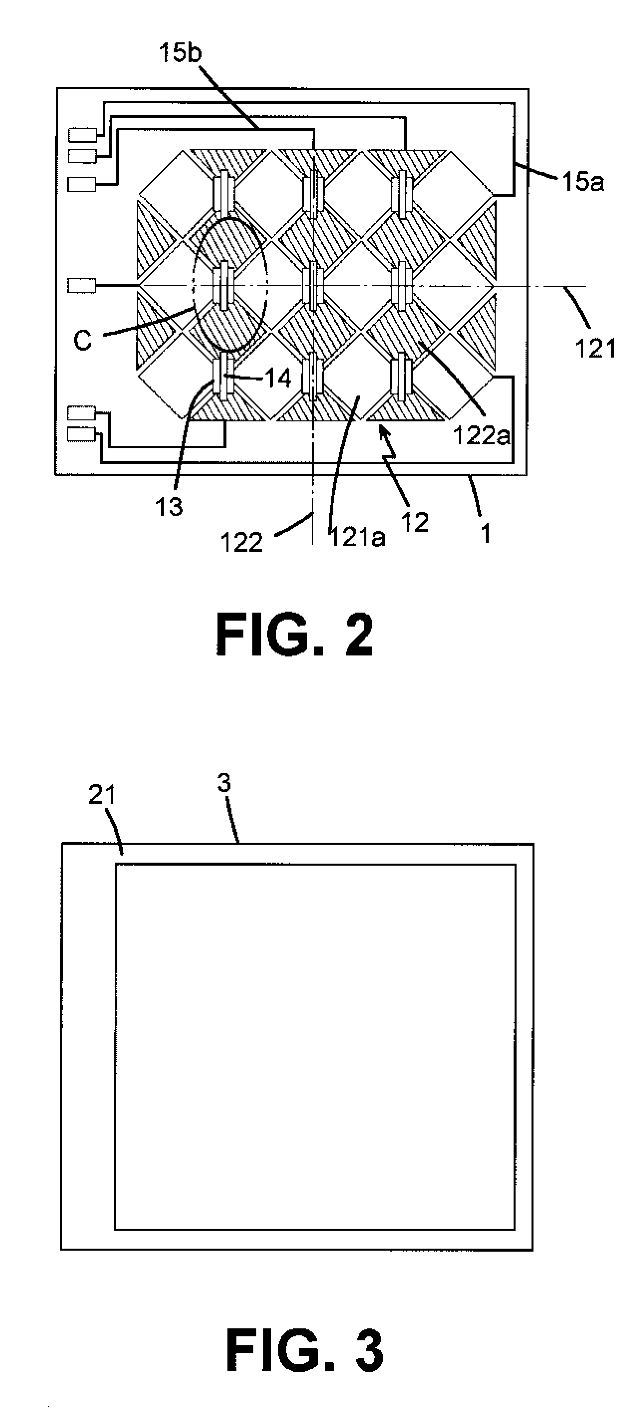
[0012]With reference to Figs. provided in the following, a capacitive touch sensing assembly according to the present invention is a plate body assembled by a bottom substrate 1 and an upper panel 2 glued by a gluing layer 3. The bottom substrate 1 and the upper panel 2 are insulated thin glasses with highly transparent property, and the gluing layer 3 is an insulated transparent UV adhesive. A colored metal-sputtered frame 21 is formed on an edge of a bottom surface of the upper panel 2. On an upper surface of the bottom substrate 1, a capacitive ...


PUM


Abstract

A capacitive touch sensing assembly is a plate body assembled by a first and second substrate glued by a gluing layer. The first and second substrates are insulated transparent thin plates, and the gluing layer is an insulated transparent adhesive. On an upper surface of the first substrate, a capacitive sensing layer including a plurality of transparent first and second axis traces intersecting to each other. Induction-spots formed on each first axis trace are connected one by one, and induction-spots formed on each second axis trace are formed separately with gaps. An inducting layer has a plurality of conducting wires formed along the direction of the second axis traces. Electrical joints formed on two ends of the conducting wires contact the two adjacent induction-spots of the second axis traces respectively so as to electrically connect all induction-spots on each second axis trace.

Description

FIELD OF THE PRESENT INVENTION[0001]The present invention relates to touch sensing assembly, and particular to a capacitive touch sensing assembly with X and Y axis traces formed on the same plane.DESCRIPTION OF THE PRIOR ART[0002]Touch panels are usually arranged in front of screens of cell phone, camera, and personal digital assistant (PDA) for operating and data input convenience. Because of advantages of stability and long life time, various types of touch panel are widely applied in products of communication, computer, and consumer. A prior capacitive touch panel includes an X axis sensing layer and a Y axis sensing layer and both of it are arranged inside the touch panel and insulated from each other. The X and Y sensing layers are grounded and connected to a control circuit respectively. When operating, an instant capacity effect is generated by a conductor or a user's finger touch so as the position being touched will be located by detection of the variation of capacitance. ...

Claims


Application Information

Patent Timeline
Patent Type & Authority Applications(United States)
IPC IPC(8): G06F3/045
CPCG06F3/044G06F2203/04111G06F3/0443G06F3/0446
Inventor LIN, TEH-ZHENG
Owner YOUNG FAST OPTOELECTRONICS
Why Eureka
Try Eureka