Method for improving electromigration lifetime of copper interconnection by extended post anneal

a technology of interconnection and electromigration lifetime, which is applied in the direction of basic electric elements, semiconductor/solid-state device manufacturing, electric apparatus, etc., can solve the problems of thinning lines, voids, and potential open circuits, and achieve the effect of reducing the electromigration of copper

Inactive Publication Date: 2010-07-01
APPLIED MATERIALS INC
View PDF13 Cites 13 Cited by
  • Summary
  • Abstract
  • Description
  • Claims
  • Application Information

AI Technical Summary

Benefits of technology

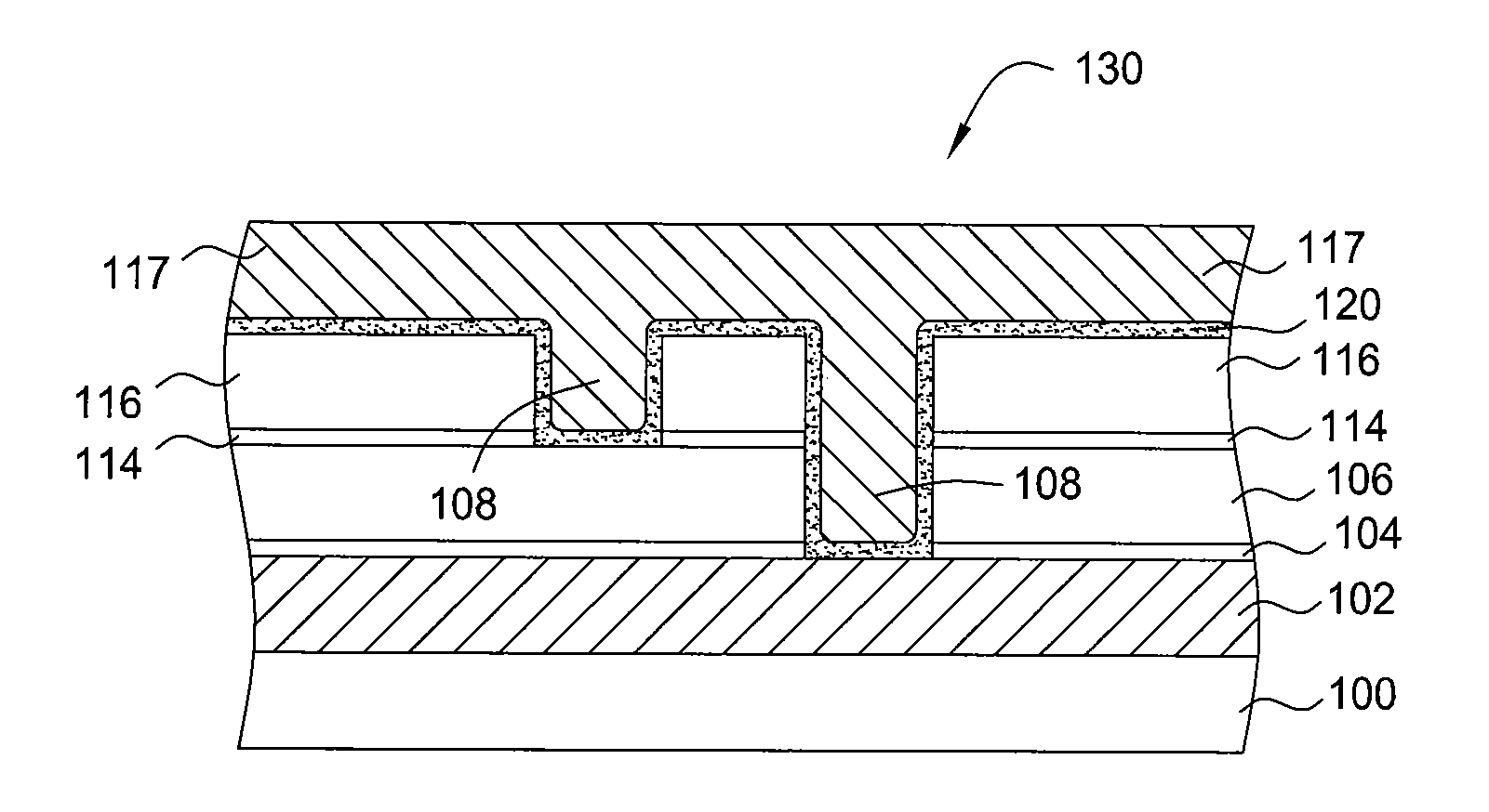
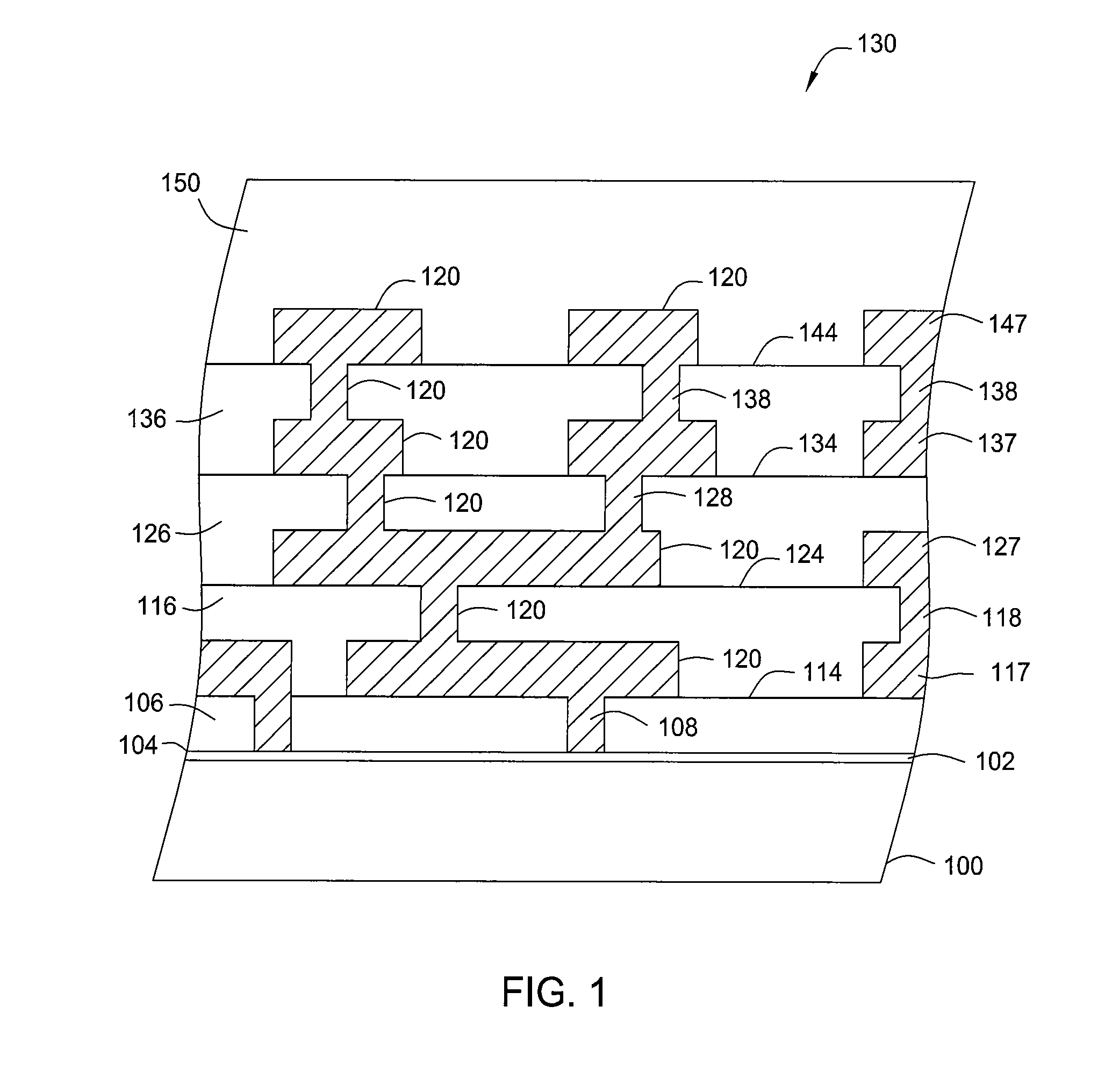
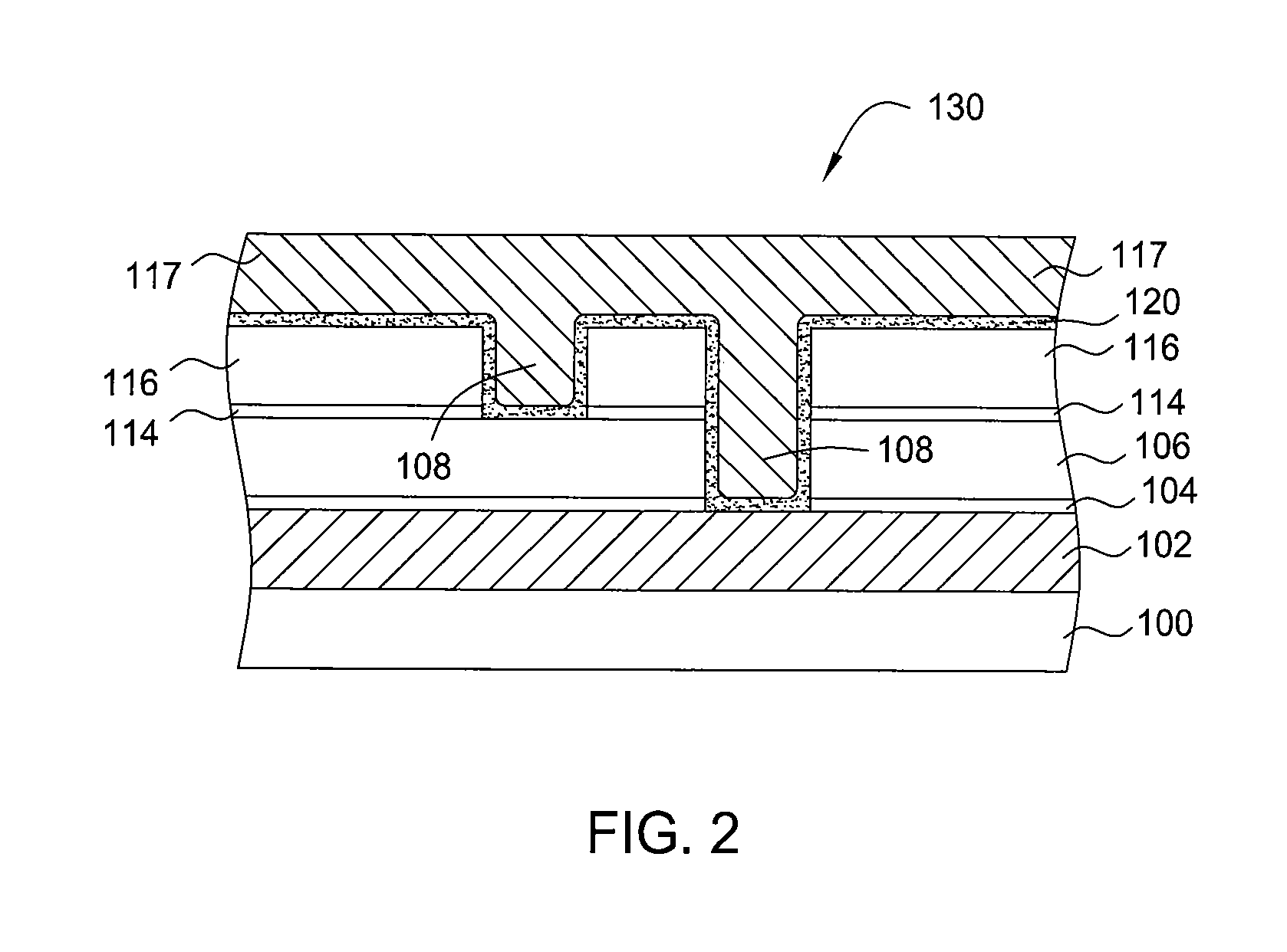
[0012]In another embodiment of the invention, a method for reducing electromigration of copper in microelectronic devices is provided. The method includes depositing a dielectric layer on a substrate; forming at least one copper interconnection structure in the dielectric layer; and annealing the copper interconnection structure at a temperature of about 150° C. to 300° C. for a time duration between about 24 to about 400 hours.

Problems solved by technology

However, with decreased feature size and the increased use of copper interconnect structures, electromigration in interconnect structures becomes a greater hurdle to overcome.
This movement may cause a depletion of atoms at the negative end of the conductor, leading to voids, thinning of lines, and a potential open circuit.
If excessive or large hillocks form, adjacent lines or lines on two levels may short together.

Method used


Image

  • Method for improving electromigration lifetime of copper interconnection by extended post anneal
  • Method for improving electromigration lifetime of copper interconnection by extended post anneal
  • Method for improving electromigration lifetime of copper interconnection by extended post anneal

Examples


example 1

[0045]In particular, microelectronic devices were formed according to the methods disclosed above. The copper interconnect structure was formed in an EnCoRe™ II processing chamber available from Applied Materials, Inc. using a barrier layer punch through process followed by a copper seed deposition process on a MTCG 65 nm e-test structure. Subsequently, the MTCG 65 nm e-test structures were subjected to an anneal at 250° C. for 168 to 336 hours.

[0046]The MTCG 65 nm e-test structures were subjected to an electromigration test by passing 1 milliAmp (mA) of current through the device in a 300° C. environment until device failure. The electromigration lifetime of the super annealed test structures (300 hours) was five times as long when compared to e-test structures not subjected to the super anneal (60 hours). Via resistances of the wafers appear to show that the longer electromigration lifetime is not due to a larger via size.

example 2

[0047]In another experiment, the copper interconnection was formed in an EnCoRe™ II processing chamber using a barrier layer punch through process followed by an RF copper deposition / etch / flash seed process on a MTCG 65 nm e-test structure. Subsequently, the MTCG e-test structures were subjected to an anneal at 250° C. for 168 to 336 hours. The MTCG 65 nm e-test structures were again subjected to an electromigration test by passing 1 mA of current through the device in a 300° C. environment until device failure. In this experiment, the electromigration lifetime of the super annealed test structures (600 hours) was still five times as long when compared to e-test structures not subjected to the super anneal (120 hours).

example 3

[0048]In another experiment, the copper interconnection was formed in an EnCoRe™ II processing chamber by an RF copper deposition / etch / flash seed process on a MTCG 65 nm e-test structure, but without the barrier layer punch through process. Subsequently, the MTCG e-test structures were subjected to an anneal at 250° C. for 168 to 336 hours. The MTCG 65 nm e-test structures were again subjected to an electromigration test with increased amperage by passing 1.5 mA of current through the device in a 300° C. environment until device failure. The electromigration lifetime of the super annealed test structures without the barrier layer punch through (180 hours) was three times as long when compared to e-test structures not subjected to the super anneal (60 hours).

[0049]The driving forces of electromigration can be described in two major categories: the electron wind force and stress gradient, such as back stress and interfacial / structural stress due to thermal expansion in confined dual-d...


PUM

PropertyMeasurementUnit
temperatureaaaaaaaaaa
feature sizeaaaaaaaaaa

Abstract

Methods for improving electromigration of copper interconnection structures are provided. In one embodiment, a method of annealing a microelectronic device includings forming microelectronic features on a substrate, forming a contact structure over the microelectronic features, and forming a copper interconnection structure over the contact structure. A passivation layer is deposited over the copper interconnection structure and the substrate is subjected to a first anneal at a temperature of about 350° C. to 400° C. for a time duration between about 30 minutes to about 1 hour. The substrate is subjected to a second anneal at a temperature of about 150° C. to 300° C. for a time duration between about 24 to about 400 hours.

Description

CROSS-REFERENCE TO RELATED APPLICATIONS[0001]This application claims benefit of U.S. provisional patent application Ser. No. 61 / 141,946, filed Dec. 31, 2008, which is herein incorporated by reference.BACKGROUND OF THE INVENTION[0002]1. Field of the Invention[0003]Embodiments of the present invention generally relate to a method of improving microelectronic device lifetime. In particular, embodiments of the present invention generally relate to improving electromigration lifetime of copper interconnection structures.[0004]2. Description of the Related Art[0005]Microelectronic devices, such as semiconductors or integrated circuits (IC), can include millions of electronic circuit devices such as transistors, capacitors, etc., such as found in ultra-large scale integrated (ULSI) circuits. To further increase the density of devices found on integrated circuits, smaller and smaller feature sizes are necessary. For example, the size of conductive lines, vias, and interconnects, gates, etc....

Claims


Application Information

Patent Timeline
Patent Type & Authority Applications(United States)
IPC IPC(8): H01L21/768
CPCH01L21/76838H01L21/76844H01L21/76855H01L21/76873H01L21/76877H01L21/76883
Inventor FU, XINYUYU, JICK M.
Owner APPLIED MATERIALS INC
Why Eureka
Try Eureka