Flash memory access circuit

a flash memory and access circuit technology, applied in the field of flash memory access circuits, can solve the problems of long access latency and relatively slow access speed, significantly slow processing, and the central processing unit cannot obtain the desired vector address stored in the vector address storage area of flash memory, so as to achieve the maximum speed of interrupt handling, without overhead, and mitigate the effect of its considerable access latency

Inactive Publication Date: 2010-07-01
KONINKLIJKE PHILIPS ELECTRONICS NV
View PDF9 Cites 28 Cited by
  • Summary
  • Abstract
  • Description
  • Claims
  • Application Information

AI Technical Summary

Benefits of technology

[0012]In an embodiment it is tested whether the copy of the instructions of the interrupt program has already been stored in the working memory before reception of the interrupt. Testing may be performed by the instruction processor itself, or for example by the memory management unit. In a further embodiment the sequence in which the instruction processor executes the instructions of the interrupt program and instructions for completing previously started access requests depends on whether the copy is found to be previously stored. If so, the instruction processor executes the instructions of the interrupt program first, but if not, the instruction processor delays loading of the copy and subsequent execution of the copy until after execution of instructions to handle of a previously started access request has been completed. In this way a maximum speed for handling the interrupt can be achieved, without the overhead of having to restart handling of previous access requests, or even losing data of such requests.
[0013]These embodiments are especially advantageous for NAND flash access, because they mitigate the effects of its considerable access latency.

Problems solved by technology

However, this comes at the expense of long access latency and a relatively slow access speed compared to state of the art RAM memory.
Control of flash memory with a main processor of a processing system can therefore significantly slow down processing.
However, if an interrupt occurs or exception handling occurs when a flash memory is used as a program memory and erasing or programming is executed for the flash memory in the user program mode or boot mode, a central processing unit cannot obtain a desired vector address stored in the vector address storage area of the flash memory.

Method used


Image

  • Flash memory access circuit
  • Flash memory access circuit
  • Flash memory access circuit

Examples


Embodiment Construction

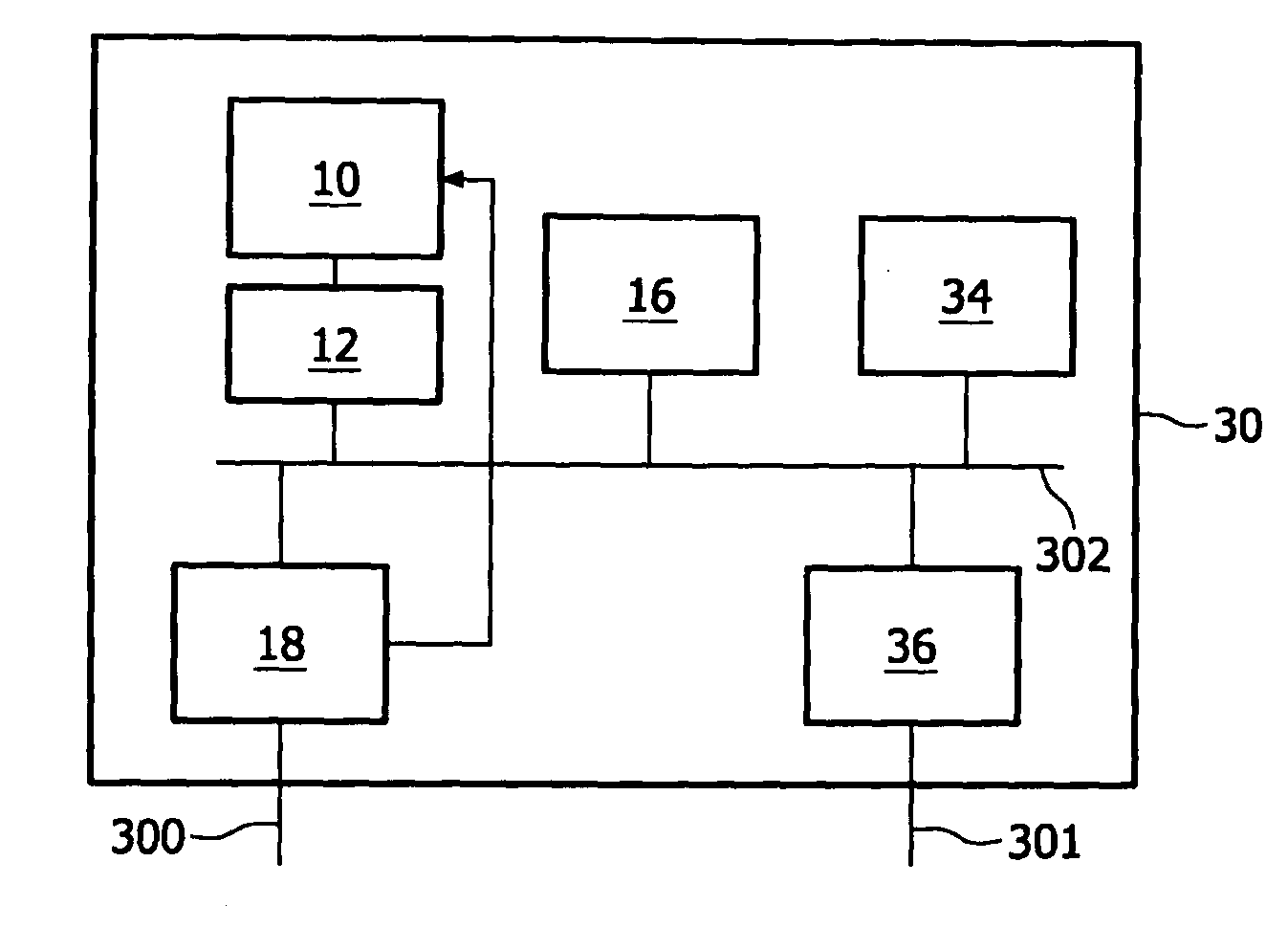
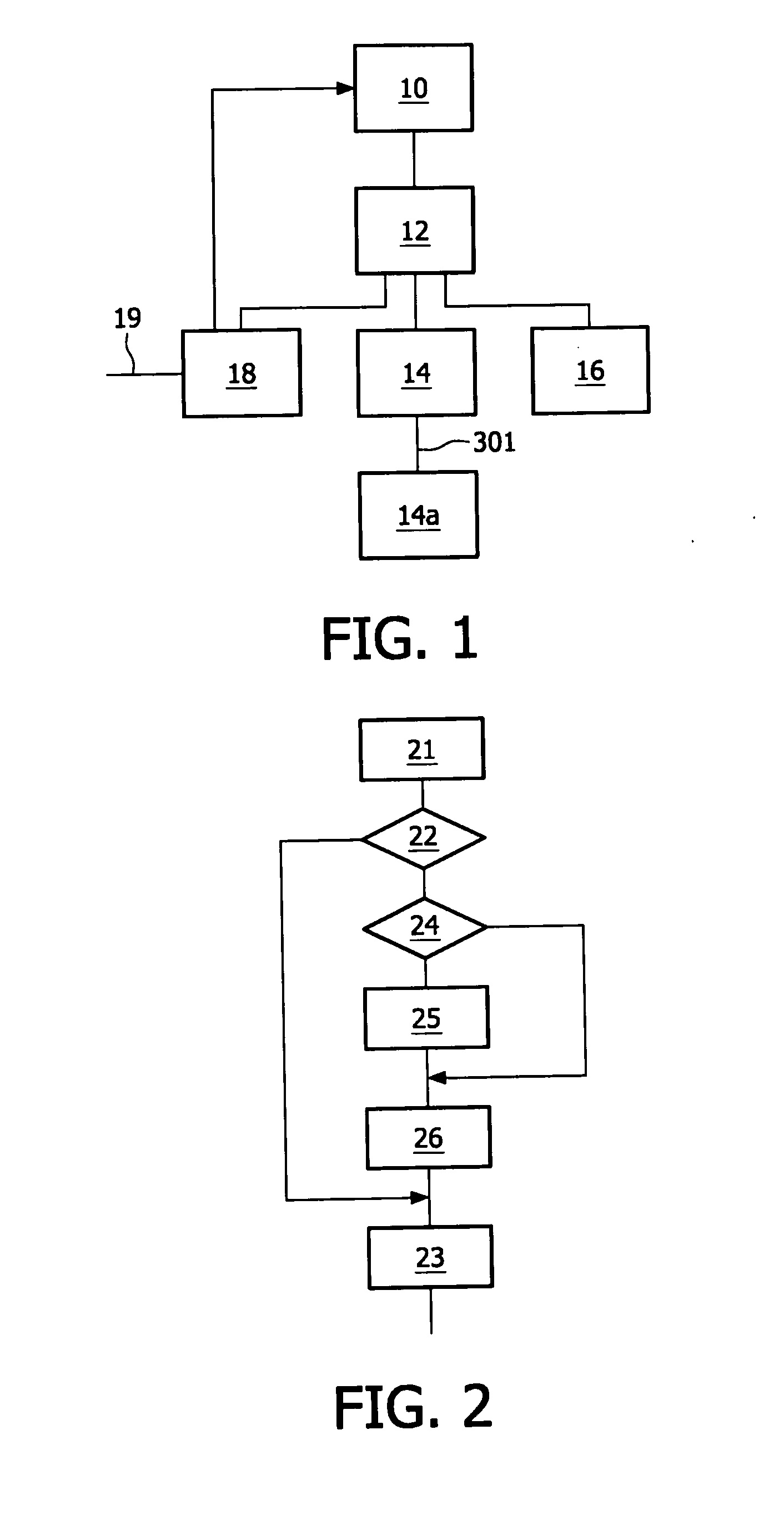
[0024]FIG. 1 shows an embodiment of a flash memory system, comprising an instruction processor 10, a memory management interface 12, a NAND flash control circuit 14, a NAND flash memory 14a, a local memory circuit 16 and a communication interface 18. Instruction processor 10 is coupled to local memory circuit 16 and a communication interface 18 via memory management interface 12. Furthermore, memory management interface 12 is coupled to NAND flash memory 14a via NAND flash control circuit 14 and a flash memory port 301. Communication interface 18 has a terminal 19 for receiving and / or transmitting information, and an output coupled to an interrupt input of instruction processor 10. Communication interface 18 may support for example communication according to the known USB (Universal Serial Bus) over terminal 19. Local memory circuit 16 may be a volatile memory circuit such as an SRAM or a DRAM. The components of the system may be integrated in an integrated circuit. In an embodiment...


PUM


Abstract

A system comprises an instruction processor (10), a flash memory device (14a), a flash control circuit (14) and a working memory (16). Instructions of an interrupt program are kept stored in the flash memory device (14a). When the instruction processor (10) receives an interrupt signal, the instruction processor (10) executes loading instructions, to cause the flash control circuit (14) to load said instructions of the interrupt program from the flash memory device (14a) into the working memory (16). The instructions of the interrupt program are subsequently executed with the instruction processor (10) from the working memory (16). Preferably it is tested whether a copy of said instructions of the interrupt program is stored in the working memory (16) at the time of the interrupt. If the copy is found stored, execution of said instructions from the copy is started before completing execution of of access instructions that were in progress at the time of the interrupt. If the copy is not found stored, execution of the access instructions is first completed and subsequently the instruction processor (10) executes the loading instructions, followed by execution of the instructions of the copy of interrupt program from the working memory (16).

Description

FIELD OF THE INVENTION[0001]The invention relates to a flash memory access circuit, and to a method of operating a flash memory access circuit.BACKGROUND OF THE INVENTION[0002]Flash memories are well known per se. Flash memory provides for high-density non-volatile memory. NAND flash in particular provides for high circuit density. However, this comes at the expense of long access latency and a relatively slow access speed compared to state of the art RAM memory. Control of flash memory with a main processor of a processing system can therefore significantly slow down processing.[0003]U.S. Pat. No. 6,874,044 discloses a flash card reader that controls transfer of data between a flash memory and a USB bus as well as some local intelligence. For transfer purposes the flash card reader contains a serial engine that interfaces to the USB bus, a flash card controller coupled to the flash memory and a RAM buffer for buffering data between the flash card controller and the serial interface...

Claims


Application Information

Patent Timeline
Patent Type & Authority Applications(United States)
IPC IPC(8): G06F12/00G06F12/02G06F13/28G06F13/24
CPCG06F9/4812
Inventor VAN ACHT, VICTOR MARTINUS GERARDUSLAMBERT, NICOLAAS
Owner KONINKLIJKE PHILIPS ELECTRONICS NV
Why Eureka
Try Eureka