Semiconductor package structure with protection bar

Active Publication Date: 2010-07-08
NAN YA TECH
View PDF14 Cites 5 Cited by
  • Summary
  • Abstract
  • Description
  • Claims
  • Application Information

AI Technical Summary

Benefits of technology

[0007]It is one objective of this invention to provide an improved semiconductor package structure in order to solve the

Problems solved by technology

A main cause for the lack of reliability in the plastic packages has been that materials having different physical characteristics are in contact with each other.
The aforesaid reliability testing is typically used to assess thermal stress and strain concentration on the solder joints between the chip and the chip carrier, which may cause potential fatigue failure of the system.
As shown in FIG. 1, the mismatch of the coefficient of thermal expansion between the chip carrier and the molding compound leads to different warping effects on the package during the thermal cycle.
When the solder joints are twitched due to compressive stress and tensile stress repeatedly concentrated thereto, the solder joints may not tightly bonded to the bond pads on a printed circuit board (PCB), causing failure of electrical connection between the package and the PCB.

Method used


Image

  • Semiconductor package structure with protection bar
  • Semiconductor package structure with protection bar
  • Semiconductor package structure with protection bar

Examples


Embodiment Construction

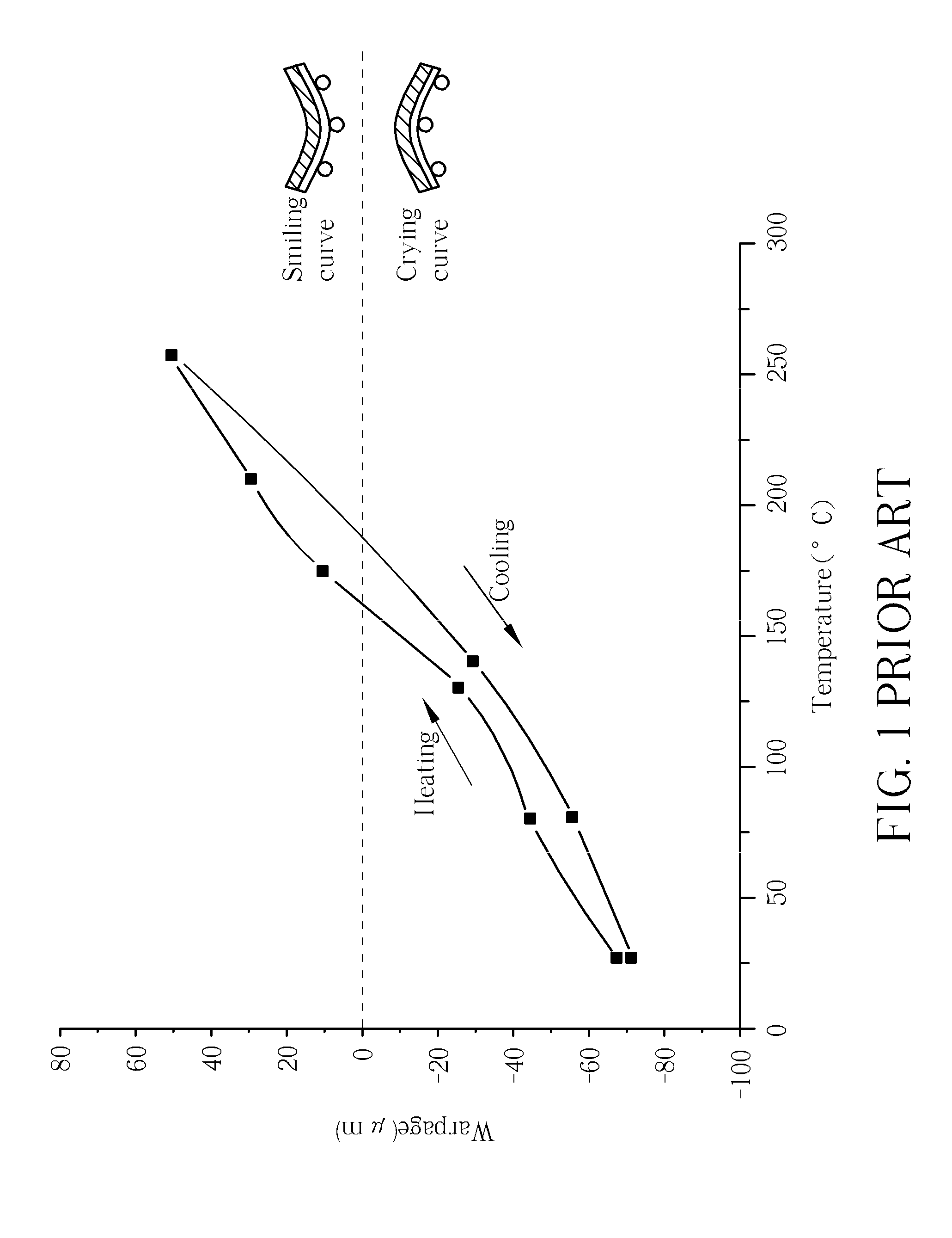
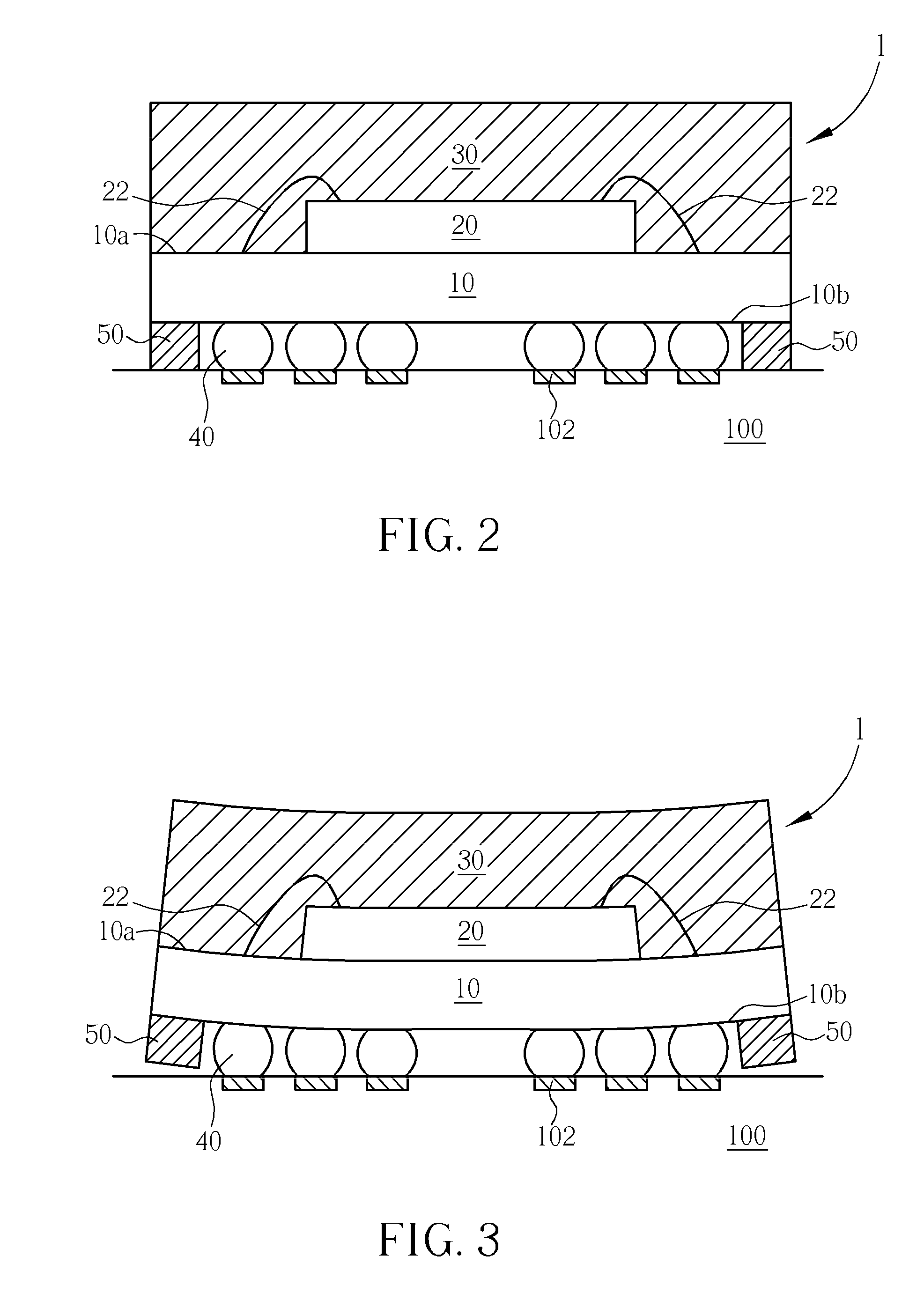
[0017]Please refer to FIG. 2 and FIG. 3. FIG. 2 is a schematic, cross-sectional diagram showing a semiconductor package structure when in a relatively low-temperature zone in accordance with one preferred embodiment of this invention. FIG. 3 is a schematic, cross-sectional diagram showing a semiconductor package structure when in a relatively high-temperature zone.

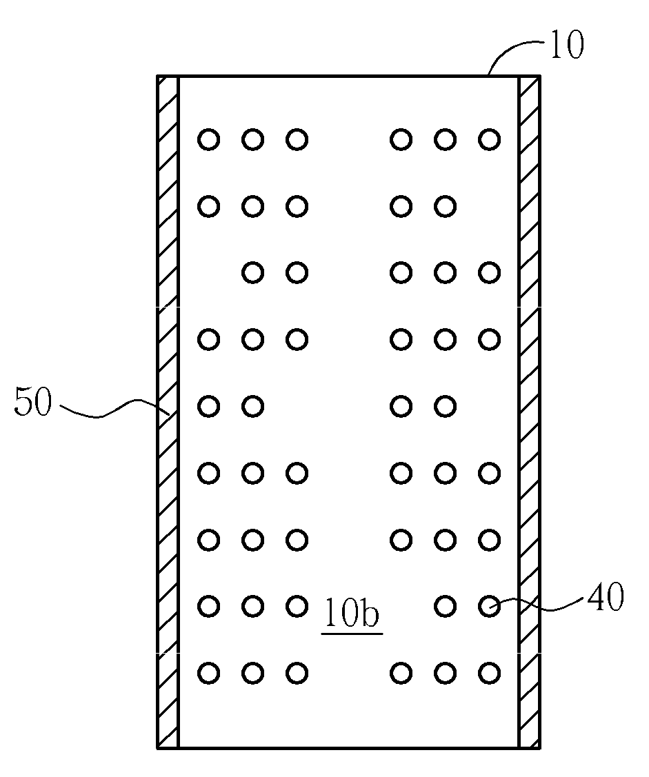
[0018]As shown in FIG. 2, the semiconductor package structure 1 comprises a carrier substrate 10. On a top surface 10a of the carrier substrate 10, there is provided an integrated circuit (IC) die 20. The IC die 20 is electrically connected with the carrier substrate 10 through a plurality of bone wires 22. The top surface 10a of the carrier substrate 10 and the IC die 20 are covered and encapsulated by a molding compound 30. On a bottom surface 10b of the carrier substrate 10, a plurality of solder balls 40 are provided. The plurality of solder balls 40 are bonded to respective bond pads 102 on a printed circuit board (PC...


PUM


Abstract

A semiconductor package structure includes a carrier, a chip or multi-chips mounted on a top surface of the carrier, a molding compound encapsulating the top surface and the chips, a plurality of solder balls distributed on a bottom surface of the carrier, and a protection bar formed of thermosetting plastic material formed on the bottom surface.

Description

BACKGROUND OF THE INVENTION[0001]1. Field of the Invention[0002]The present invention relates to a semiconductor package structure. More particularly, the present invention relates to a semiconductor package structure with a protection bar that can prevent package warpage.[0003]2. Description of the Prior Art[0004]There are continuing efforts to improve the reliability of the plastic package technology for encapsulating semiconductor devices. A main cause for the lack of reliability in the plastic packages has been that materials having different physical characteristics are in contact with each other. For example, differences in coefficient of thermal expansion among a molding compound which forms the package body, a semiconductor chip which is made of silicon, and solder balls consisting of tin alloy, can cause separation of the materials during subsequent reliability testing. The aforesaid reliability testing is typically used to assess thermal stress and strain concentration on ...

Claims


Application Information

Patent Timeline
IPC IPC(8): H01L23/50H01L25/03
CPCH01L23/3128H01L23/562H01L2224/48225H01L2924/12044H01L2924/15311H01L24/48H01L2224/48227H01L2924/14H01L2924/00H01L2924/181H01L2924/3511H01L2924/00012H01L2924/00014H01L2224/45099H01L2224/45015H01L2924/207
Inventor CHEN, JEN-CHUNG
Owner NAN YA TECH
Why Eureka
Try Eureka