Layout verification device, layout verification program, and layout verification method of layout pattern of semiconductor device
- Summary
- Abstract
- Description
- Claims
- Application Information
AI Technical Summary
Benefits of technology
Problems solved by technology
Method used
Image
Examples
first exemplary embodiment
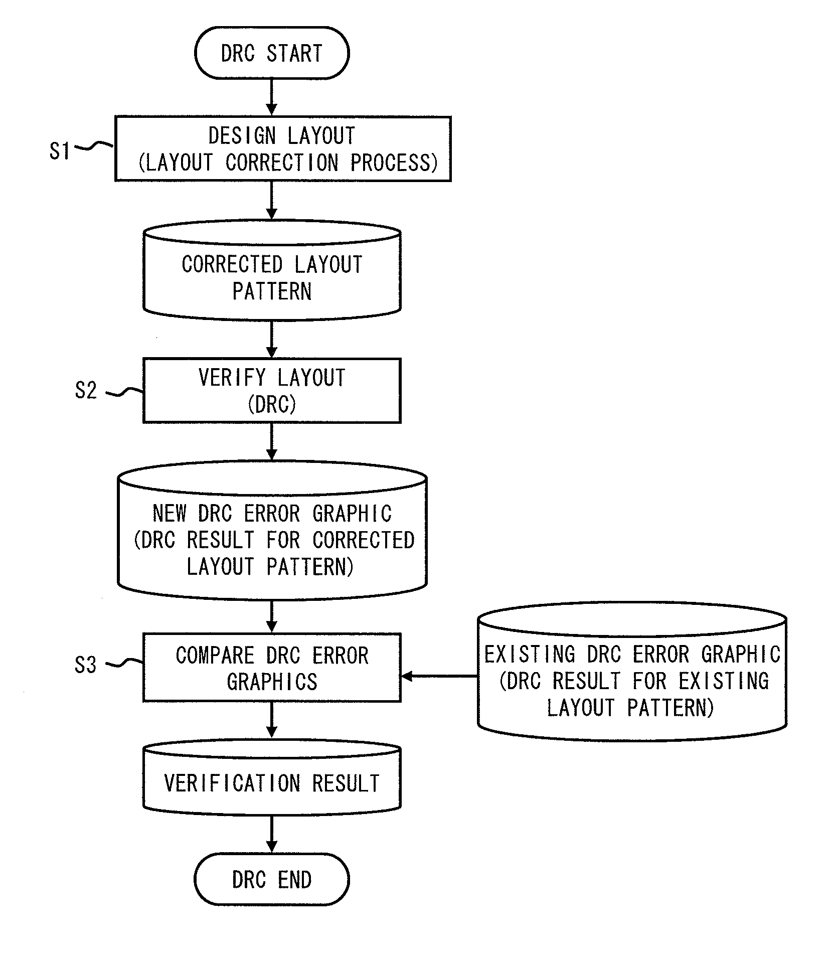
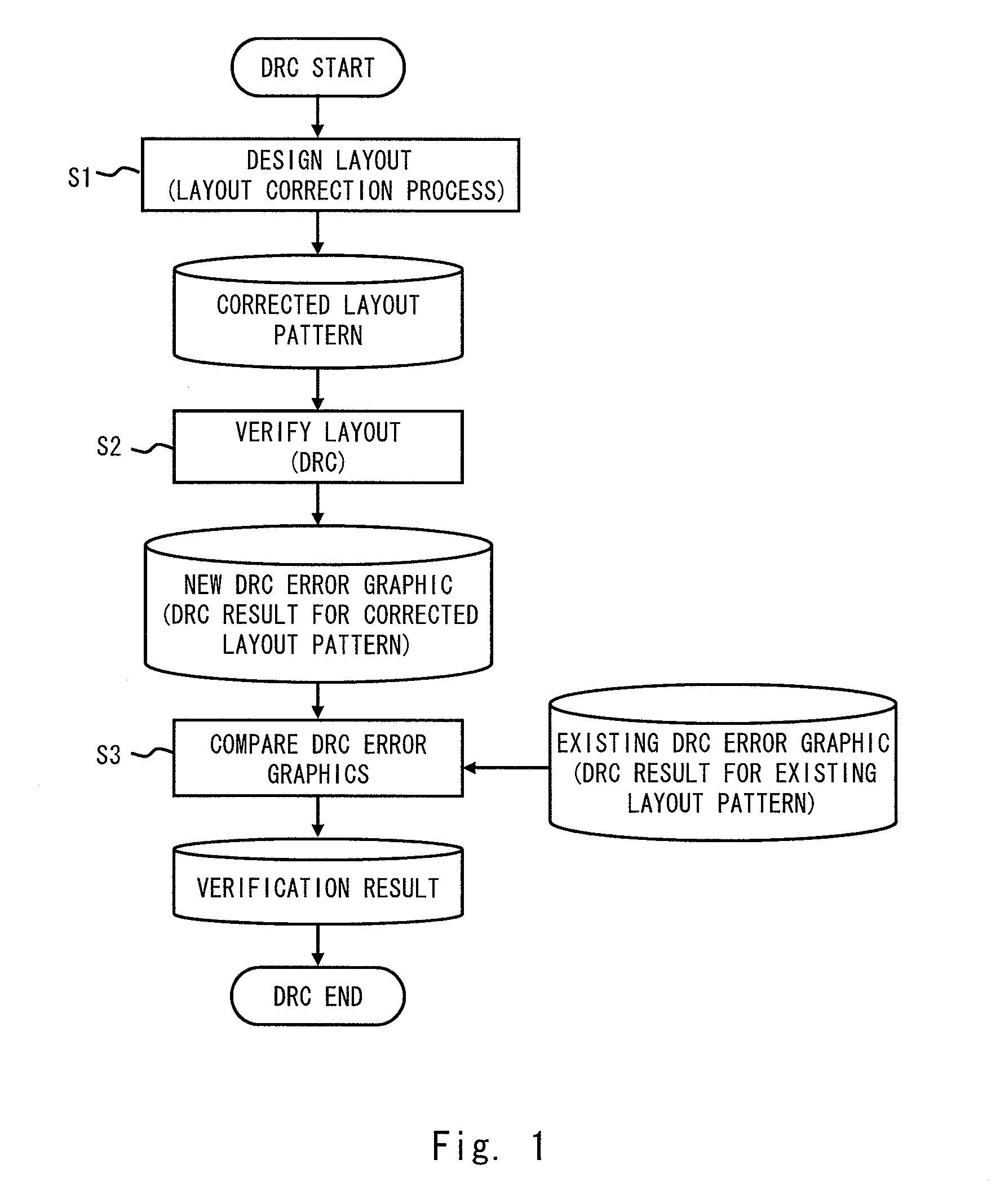
[0038]Hereinafter, the exemplary embodiments of the present invention will be described with reference to the drawings. A layout verification method according to the first exemplary embodiment may be realized as a hardware (layout verification device), or may be realized as a software (layout verification program) that operates on a calculation circuit such as a CPU (Central Processing Unit) or the like. In the following description, the layout verification method will be described first, and thereafter a method of realizing the layout verification method according to the first exemplary embodiment in the hardware or the software will be described.
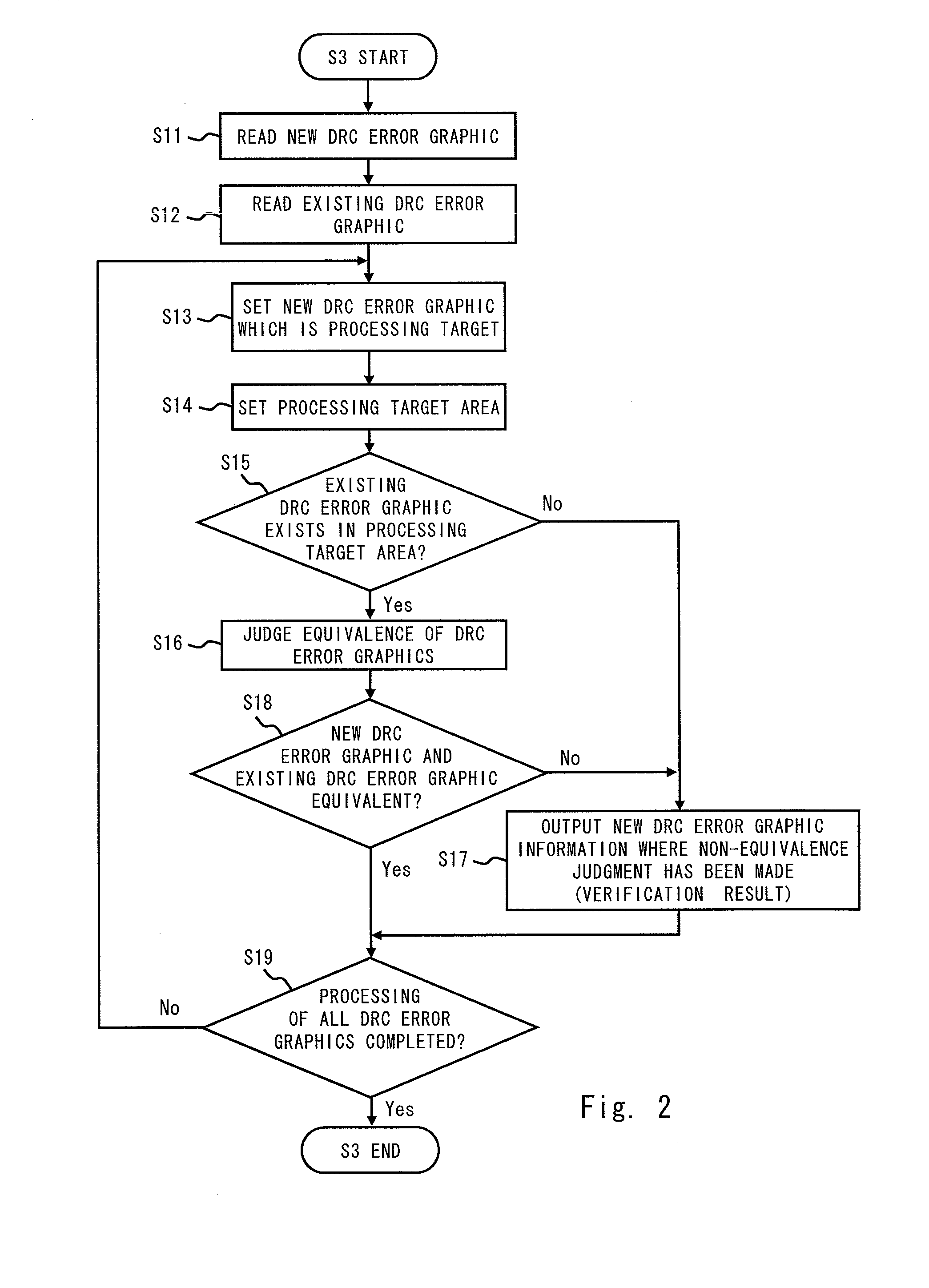
[0039]Further, the layout verification method according to the first exemplary embodiment is employed in order to remove a pseudo error that is already verified among pseudo errors included in an error graphic output in a DRC (Design Rule Check) verification process included in a layout process. Thus, in the layout process that is performe...
second exemplary embodiment
[0075]In the second exemplary embodiment, a method of limiting the number of peripheral vertex coordinates that are the comparison target in step S35 shown in FIG. 4 to two is described. FIGS. 12 and 13 show schematic diagrams of the peripheral vertex coordinates set in the layout verification method of the second exemplary embodiment.
[0076]In the example shown in FIG. 12, the vertex D1 which is the target vertex coordinate in the new DRC error graphic is located on a side of the wiring W2. In such a case, the grid intersection where the vertex D1 may be deviated is limited to the side where the vertex D1 is located in the wiring W2. In the example shown in FIG. 12, only the peripheral vertex coordinates F4 and F5 that are set to the grid intersections on the side of the wiring W2 where the vertex D1 is located are comparison candidates.
[0077]Further, in the example shown in FIG. 13, the vertex D1 which is the target vertex coordinate in the new DRC error graphic is located at a cor...
third exemplary embodiment
[0079]In the third exemplary embodiment, a method of limiting the number of peripheral vertex coordinates that are comparison target in step S35 shown in FIG. 4 to one will be described. FIGS. 14 and 15 show schematic diagrams of the peripheral vertex coordinates set in the layout verification method of the third exemplary embodiment.
[0080]In the example shown in FIG. 14, the vertex D1 which is the target vertex coordinate in the new DRC error graphic is located on the side of the wiring W2. Further, in the example shown in FIG. 14, the vertex D2 corresponding to the vertex D1 in the existing DRC error graphic exists on the side that connects the vertex D1 and the vertex B in the wiring W2. Thus, the grid intersection where the vertex D1 may be deviated is limited to the side that connects the vertex D1 and the vertex B in the wiring W2. Thus, in the example shown in FIG. 14, only the peripheral vertex coordinate F5 set to the grid intersection on the side of the wiring W2 where the...
PUM
 Abstract
Description
Claims
Application Information


