Rewritable memory device

a memory device and rewritable technology, applied in semiconductor devices, digital storage, instruments, etc., can solve the problems of data error, similar problems can arise in other types of programmable resistance materials, and not many memory cell technologies can meet both of these requirements, so as to facilitate asymmetrical segregation/re-absorption processes, and enhance electromigration and other kinetic processes.

Active Publication Date: 2010-07-15
TAIWAN SEMICON MFG CO LTD +1
View PDF99 Cites 13 Cited by
  • Summary
  • Abstract
  • Description
  • Claims
  • Application Information

AI Technical Summary

Benefits of technology

[0016]In embodiments the second bias arrangement may have opposite polarity to that of the first bias arrangement, to enhance electromigration and other kinetic processes that are dependent upon the direction of the applied electric field and/or current.
[0017]In embo

Problems solved by technology

However, not many memory cell technologies can satisfy both of these requirements.
If these crystalline regions connect to form a low resistance path through the active region,

Method used


Image

  • Rewritable memory device
  • Rewritable memory device
  • Rewritable memory device

Examples


Embodiment Construction

[0040]A detailed description of embodiments of the present invention is provided with reference to the FIGS. 1-21.

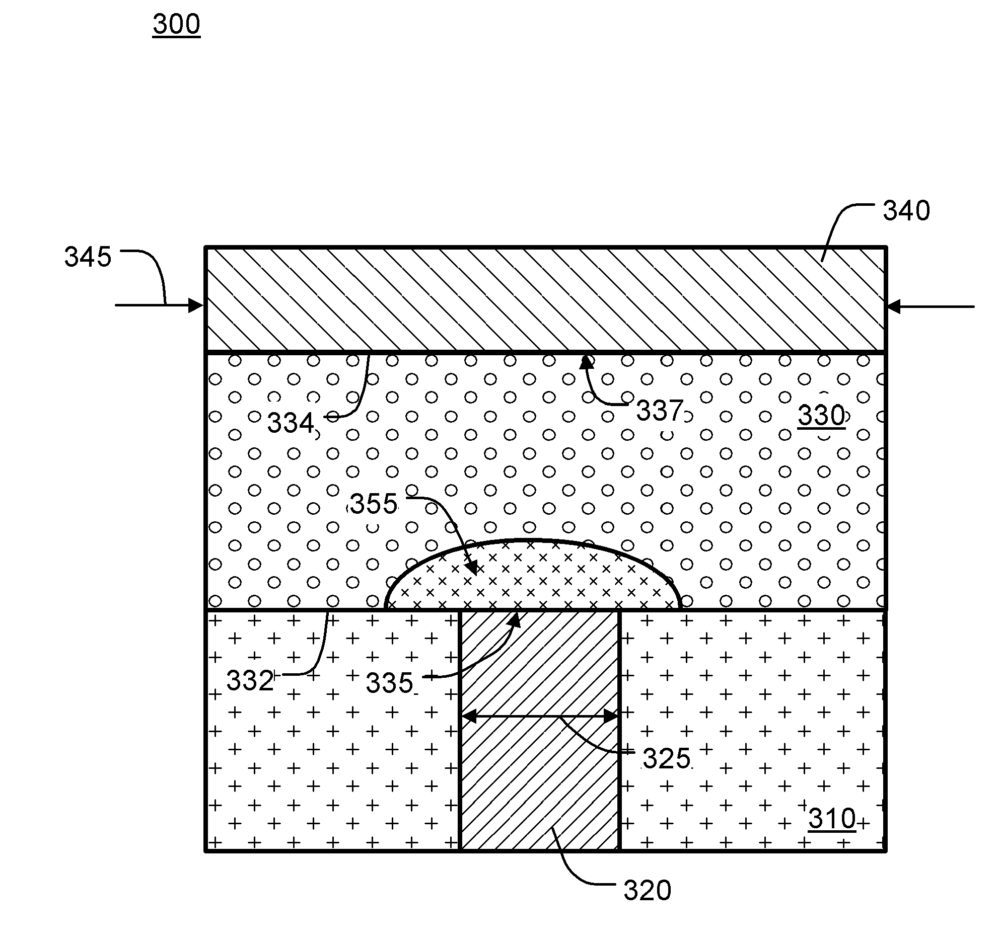
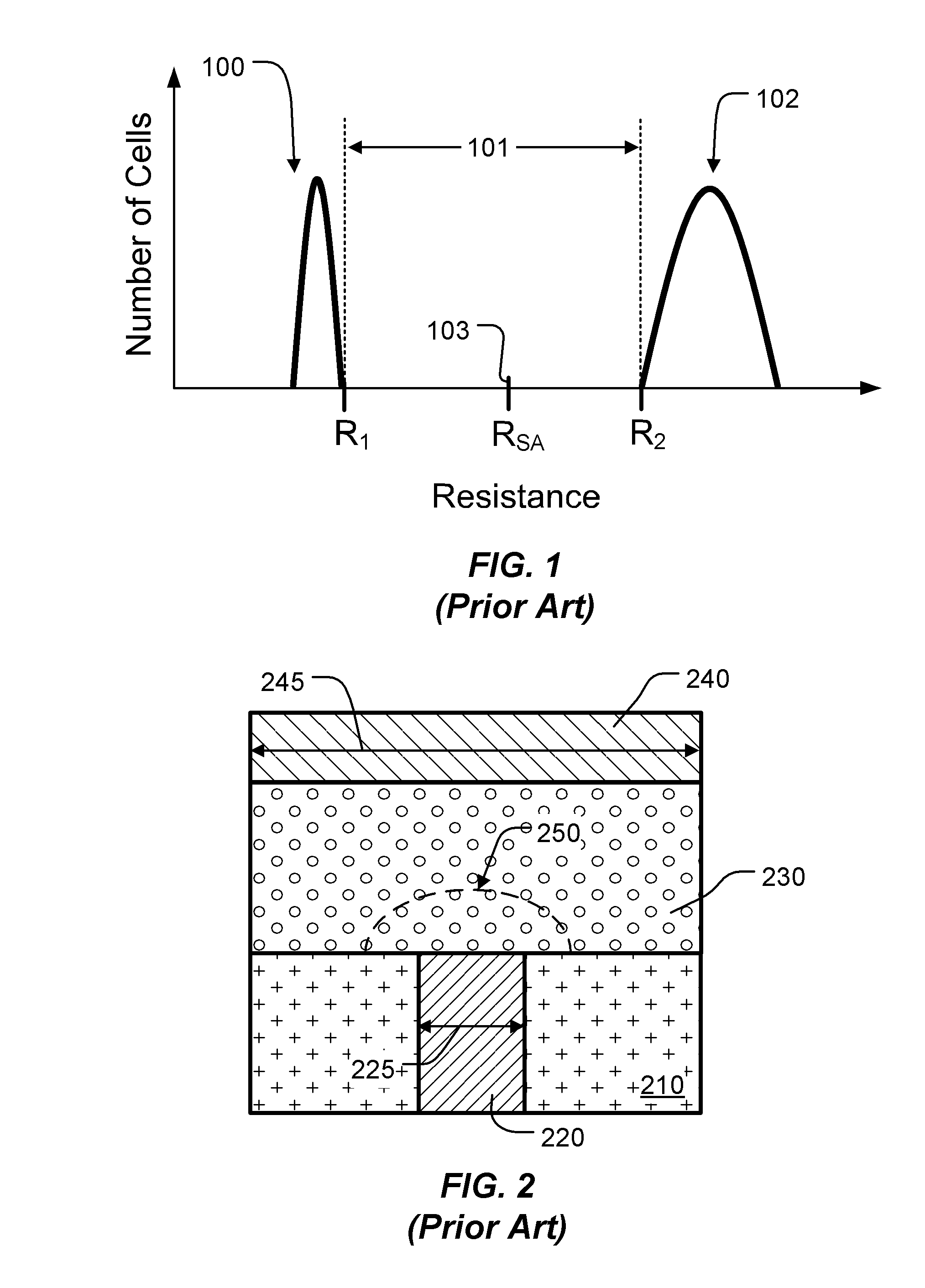
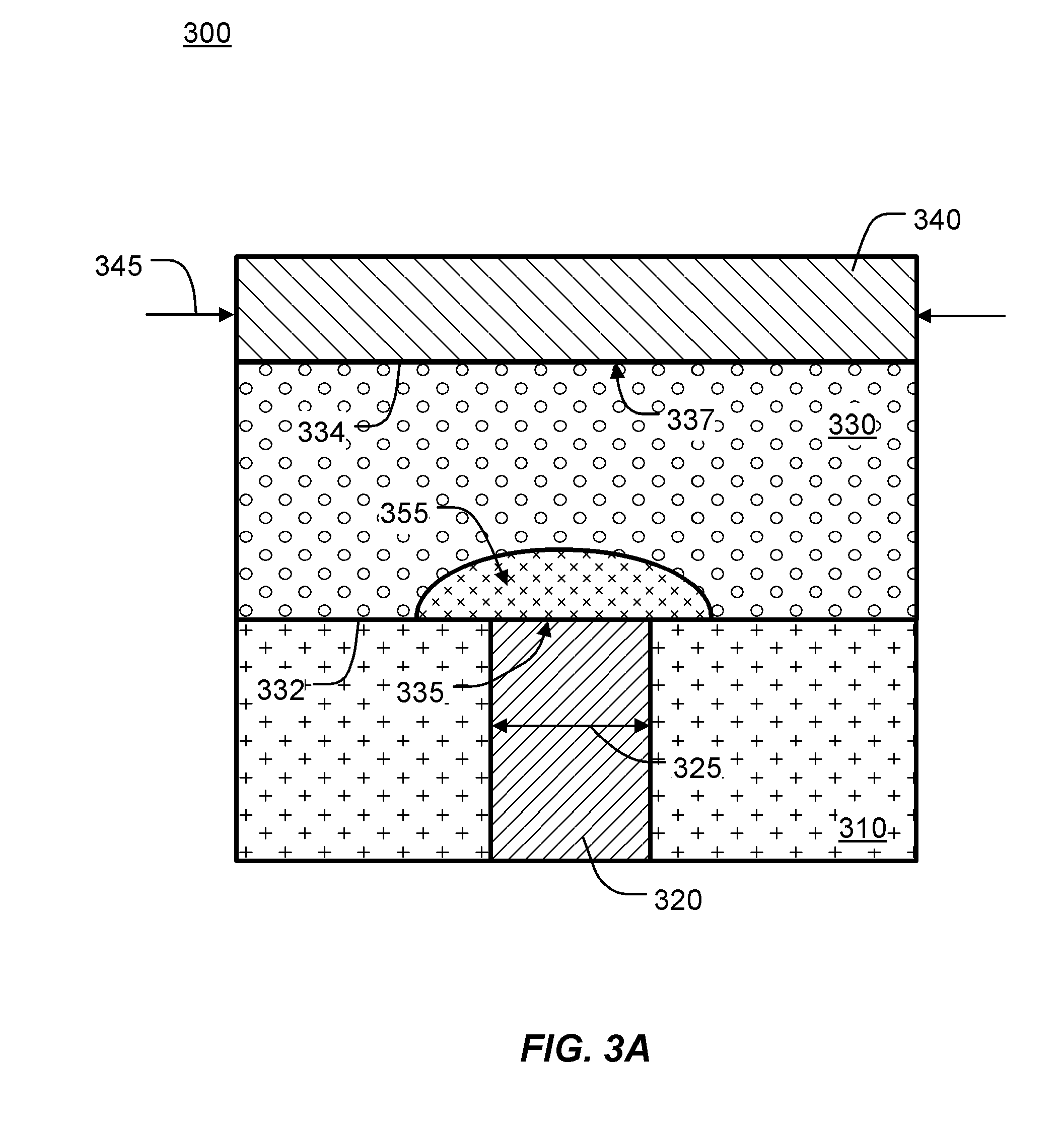
[0041]In conventional phase change memory, data is stored by causing transitions in an active region of the phase change material between amorphous and crystalline phases, which have significantly different resistances. FIG. 1 is a graph of resistance distribution for memory states in memory cells storing a single bit of data, including a lower resistance set (programmed) state 100 corresponding to a primarily crystalline phase in the active region of the cell, and a high resistance reset (erased) state 102 corresponding to a primarily amorphous phase in the active region of the cell. For reliable operation, the resistance distributions must have non-overlapping resistance ranges.

[0042]The difference between the highest resistance R1 of the lower resistance state 100 and the lower resistance R2 of the high resistance reset state 102 defines a read margin 101 used to dist...


PUM


Abstract

Memory devices described herein are programmed and erased by physical segregation of an electrically insulating layer out of a memory material to establish a high resistance state, and by re-absorption of at least a portion of the electrically insulating layer into the memory material to establish a low resistance state. The physical mechanism of programming and erasing includes movement of structure vacancies to form voids, and/or segregation of doping material and bulk material, to create the electrically insulating layer consisting of voids and/or dielectric doping material along an inter-electrode current path between electrodes.

Description

CROSS-REFERENCE TO RELATED APPLICATIONS[0001]This application claims the benefit of U.S. Provisional Patent Application No. 61 / 144,692 titled “Rewritable Memory Device” filed on 14 Jan. 2009, which is incorporated by reference herein.PARTIES TO A JOINT RESEARCH AGREEMENT[0002]International Business Machines Corporation, a New York corporation, and Macronix International Corporation, Ltd., a Taiwan corporation, are parties to a Joint Research Agreement.BACKGROUND OF THE INVENTION[0003]1. Field of the Invention[0004]The present invention relates to programmable resistance memory devices, and methods for operating such devices.[0005]2. Description of Related Art[0006]Many electronic systems need a nonvolatile memory having very long retention times at high temperature, and yet are also rewritable for updating codes and data stored therein. However, not many memory cell technologies can satisfy both of these requirements.[0007]Phase change based memory materials, like chalcogenide based...

Claims


Application Information

Patent Timeline
IPC IPC(8): G11C11/00H01L47/00G11C11/34
CPCG11C13/0004G11C13/0069G11C2013/0071G11C2013/009G11C2013/0092H01L45/1625G11C2213/79H01L45/08H01L45/1233H01L45/144G11C2213/33
Inventor LEE, MING-HSIUCHEN, CHIEH-FANGSHIH, YEN-HAOZHU, YU
Owner TAIWAN SEMICON MFG CO LTD
Why Eureka
Try Eureka