Semiconductor devices with copper interconnects and composite silicon nitride capping layers

Active Publication Date: 2009-05-19
ADVANCED MICRO DEVICES INC
View PDF9 Cites 10 Cited by
  • Summary
  • Abstract
  • Description
  • Claims
  • Application Information

AI Technical Summary

Benefits of technology

[0008]An advantage of the present invention is a method of manufacturing semiconductor memory devices with improved data retention, and comprising reliably capped Cu or Cu alloy interconnects with reduced interconnect capacitance, improved electromigration and improved capping layer adhesion.
[0009]Another advantage of the present invention is a semiconductor memory device exhibiting improved data retention and comprising reliably capped Cu or Cu alloy interconnects exhibiting reduced electromigration and improved capping layer adhesion.
[0010]Additional advantages and other features of the present invention will be set forth in the description which follows and in part will be apparent to those having ordinary skill in the art upon examination of the following or may be learned from the practice of the present invention. The advantages of the present invention may be realized and obtained as particularly pointed out in the appended claims.
[0011]According to the present invention, the foregoing and other advantages are achieved in part by a semiconductor device comprising: a layer of copper (Cu); a first silicon nitride layer, having a first silicon-hydrogen bond (Si—H) concentration, on the layer of Cu; and a second silicon nitride layer, having a second Si—H concentration less than the first Si—H concentration, on a first-silicon nitride layer.
[0012]Another advantage of the present invention is a method of fabricating a semiconductor device, the method comprising: depositing a layer of copper (Cu); depositing a

Problems solved by technology

As device dimensions shrink into the deep sub-micron regime, vulnerability to mobile ion contamination, such as hydrogen degradation, increases.
The inability to adequately getter mobile ion contaminants, such as hydrogen ions, results in a neutralization of electrons and, hence, leakage causing programming loss as well as a charge gain causing reappearance of erased information.
The technological benefits of Cu, such as reduced R×C delay are clear; however, various reliability issues have evolved.
There are additional problems attendant upon conventional Cu interconnect methodology employing a diffusion barrier layer (capping layer).
It was found, however, that capping layers, such as silicon nitride, deposited by plasma enhanced chemical vapor deposition (PECVD), exhibit poor adhesion to the Cu or Cu alloy surface.
Consequently, the capping layer is vulnerable to removal, as by peeling due to scratching or stresses re

Method used


Image

  • Semiconductor devices with copper interconnects and composite silicon nitride capping layers
  • Semiconductor devices with copper interconnects and composite silicon nitride capping layers
  • Semiconductor devices with copper interconnects and composite silicon nitride capping layers

Examples


Embodiment Construction

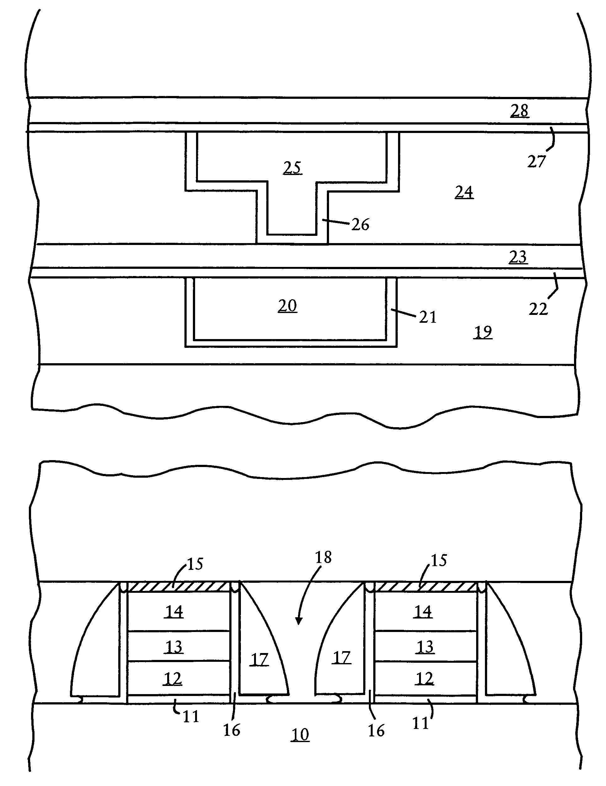
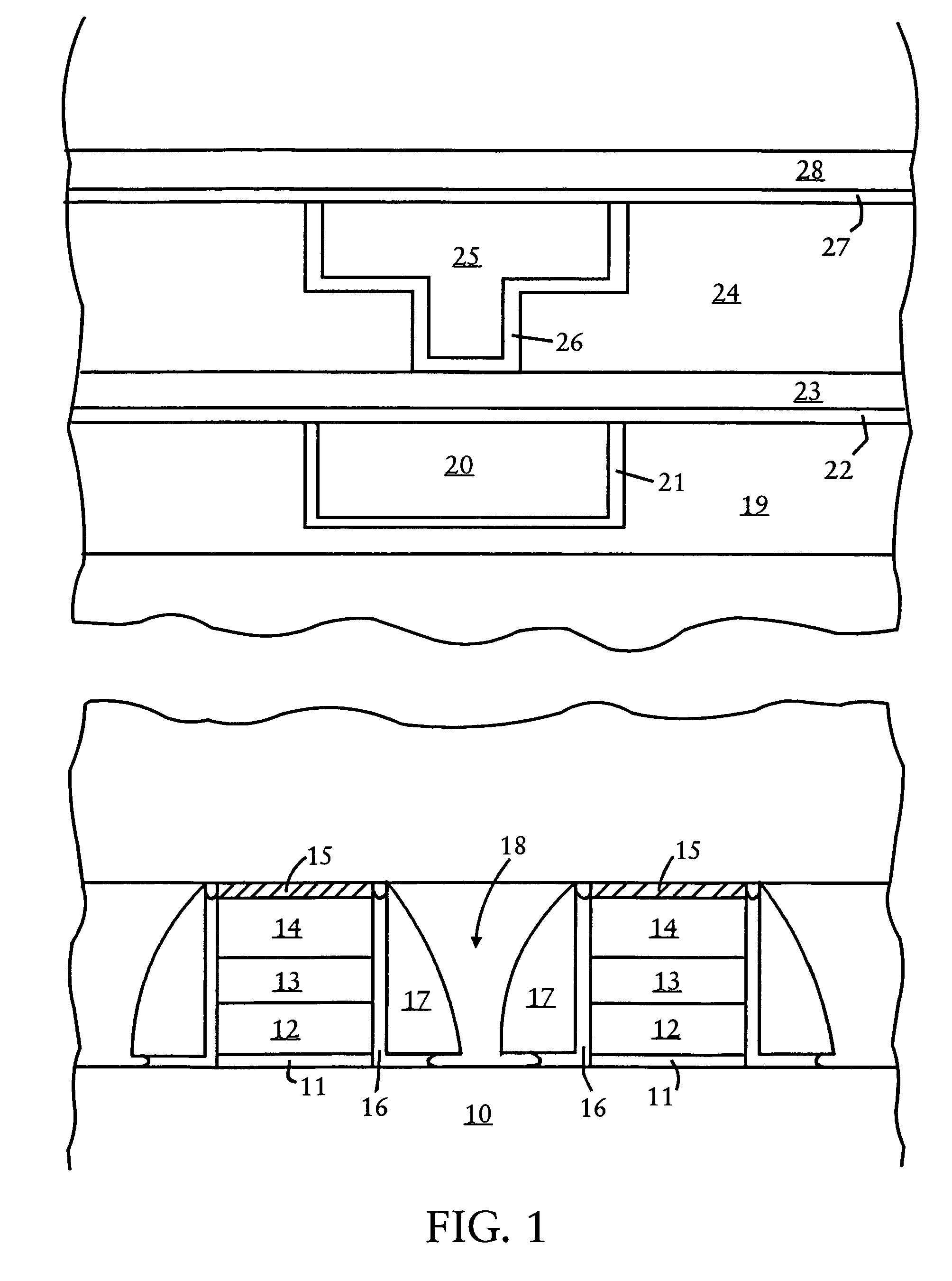
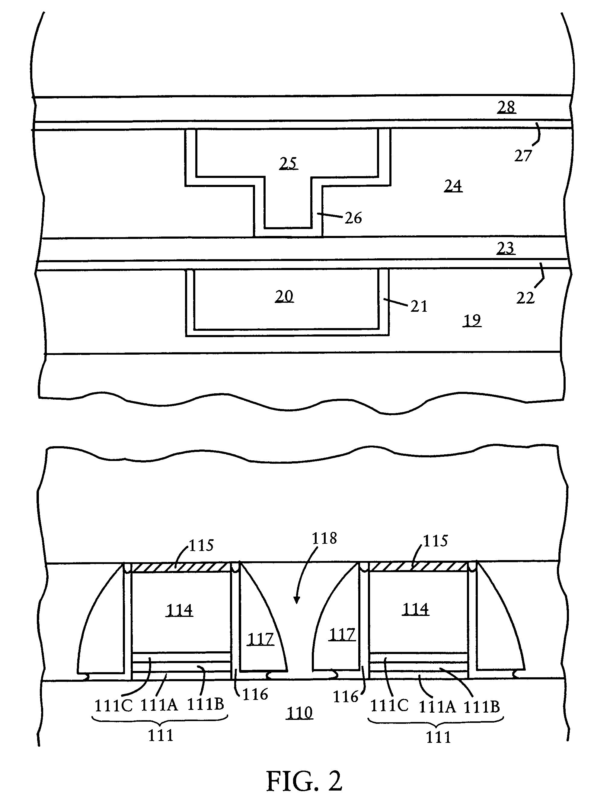
[0018]The present invention addresses and solves various reliability problems attendant upon conventional semiconductor fabrication techniques. These problems arise as semiconductor memory device dimensions continue to shrink, making it increasingly more difficult to effectively getter mobile ion contaminants, such as hydrogen. The hydrogen contamination problem becomes exacerbated when integrating copper interconnect technology with flash memory devices. It was found that conventionally deposited silicon nitride capping layers exhibit a relatively high degree of Si—H bonding, such as about 0.3% to about 0.9%, thereby generating charge loss problems for miniaturized flash technology. It was also found that the conventionally deposited silicon nitride layers do not adequately adhere to inlaid copper subsequent to implementing Cu CMP processing, even when the Cu surface is treated with an ammonia plasma. Such poor adhesion exacerbates electromigration issues.

[0019]The present inventio...


PUM

PropertyMeasurementUnit
Fractionaaaaaaaaaa
Fractionaaaaaaaaaa
Fractionaaaaaaaaaa

Abstract

Cu interconnects are formed with composite capping layers for reduced electromigration, improved adhesion between Cu and the capping layer, and reduced charge loss in associated non-volatile transistors. Embodiments include depositing a first relatively thin silicon nitride layer having a relatively high concentration of Si—H bonds on the upper surface of a layer of Cu for improved adhesion and reduced electromigration, and depositing a second relatively thick silicon nitride layer having a relatively low concentration of Si—H bonds on the first silicon nitride layer for reduced charge loss.

Description

FIELD OF THE INVENTION[0001]The present invention relates to copper (Cu) and / or Cu alloy metallization in semiconductor devices, and to a method for forming reliably capped Cu or Cu alloy interconnects. The present invention is particularly applicable to manufacturing high-speed integrated circuits in semiconductor memory devices, particularly flash memory devices, with reduced charge loss, reduced electromigration and improved capping layer adhesion.BACKGROUND OF THE INVENTION[0002]Semiconductor memory devices, such as erasable, programmable, read-only memories (EPROMs), electrically erasable programmable read-only memories (EEPROMs), and flash erasable programmable read-only memories (FEPROMs) are erasable and reusable, and are employed in various commercial electronic devices, such as computers, cellular telephones and digital cameras. There has recently evolved devices termed mirrorbit devices which do not contain a floating gate electrode. In mirrorbit devices, the gate electro...

Claims


Application Information

Patent Timeline
IPC IPC(8): H01L21/4763H01L21/31H01L21/44
CPCC23C16/345H01L21/3185H01L21/76832H01L21/76834H01L27/11521H01L27/11568H01L21/02274H01L21/022H01L21/02211H01L21/0217H10B41/30H10B43/30
Inventor NGO, MINH VANWILSON, ERIKPHAM, HIEUHUERTAS, ROBERTYOU, LUTOKUNO, HIROKAZUNICKEL, ALEXANDERTRAN, MINH
Owner ADVANCED MICRO DEVICES INC
Why Eureka
Try Eureka