Semiconductor device and manufacturing method thereof

a technology of semiconductor devices and manufacturing methods, applied in semiconductor devices, semiconductor/solid-state device details, electrical apparatus, etc., can solve the problems of increasing resistance value between plugs and wires, and achieve the effects of suppressing metal added diffusion, improving stress migration resistance and electromigration resistance, and suppressing metal oxide film formation

Inactive Publication Date: 2007-06-28
PANASONIC CORP +1
View PDF1 Cites 10 Cited by
  • Summary
  • Abstract
  • Description
  • Claims
  • Application Information

AI Technical Summary

Benefits of technology

[0018] An object of the invention is to provide a semiconductor device without the above-mentioned problems, the semiconductor device being manufactured with a good yield and having high reliability and another object of the invention is to provide a manufacturing method of such semiconductor device.
[0021] In this structure, the second metal film containing metal having the binding energy with oxygen lower than that of the first metal film is provided between the first metal film and the copper film. Metal having the binding energy with oxygen lower than that of the first metal film is diffused from the first metal film into the copper film by a thermal treatment performed in a manufacturing process. However, in this structure, it is possible to reduce the amount of the metal having the binding energy with oxygen lower than that of the first metal film. As a result, it is possible to reduce a thickness of the metal oxide film to be formed by the thermal treatment on the upper surface of the copper film compared to the conventional structure, and it is possible to reduce the resistance value between the plug and the wire.
[0023] In this method, it is possible to improve stress migration resistance and electromigration resistance by adding metal having the binding energy with oxygen higher than that of the copper to a material for the first metal film, and at the same time, it is possible to suppress the formation of the metal oxide film on the upper surface of the copper film by suppressing the diffusion of the metal added to the material for the first metal film. By this method, it is possible to reduce the resistance between the plug and the copper film, so that it is possible to manufacture semiconductor device with improved reliability and with a good yield.

Problems solved by technology

However, the structure of the above-mentioned conventional semiconductor device and the manufacturing method have a problem that the resistance value between a plug and a wire may increase.

Method used


Image

  • Semiconductor device and manufacturing method thereof
  • Semiconductor device and manufacturing method thereof
  • Semiconductor device and manufacturing method thereof

Examples


embodiment

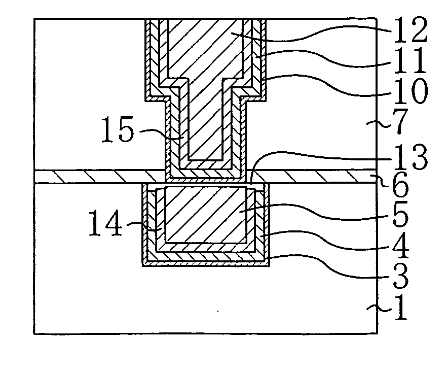
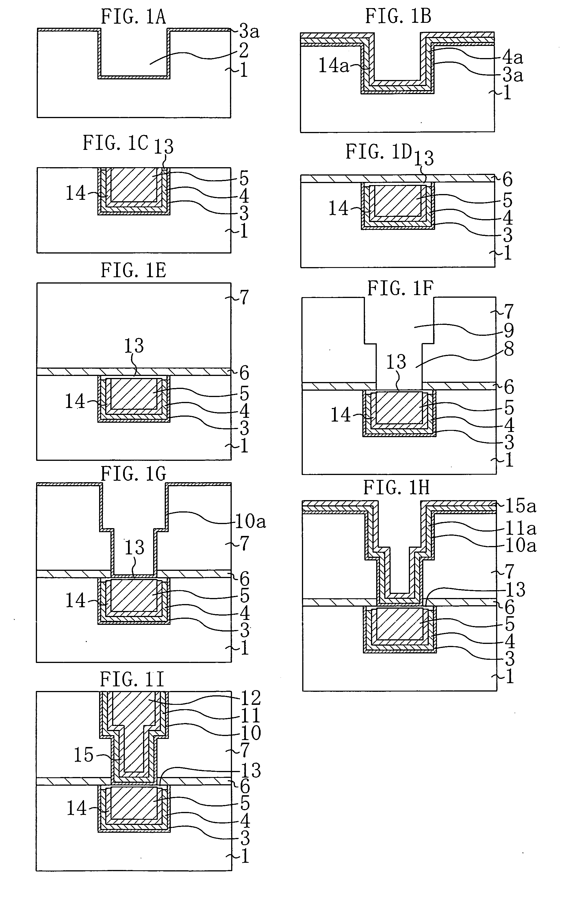
[0029]FIGS. 1A through 1I are cross sections illustrating a semiconductor device manufacturing method according to an embodiment of the present invention.

[0030] First, referring to FIG. 1A, a lithography step and an etching step is performed so as to form a first wire trench 2 in a first interlayer dielectric film 1, the first interlayer dielectric film 1 being formed of a low dielectric constant material on a substrate (not shown). Next, as a preparatory process, an annealing process is performed on the substrate (semiconductor device) for 60 seconds in a hydrogen atmosphere at a temperature of 280° C. so as to reduce an oxide film formed on a surface of the semiconductor device. Then, as a barrier metal film 3a, a tantalum nitride film having a thickness of 5 nm and a tantalum film having a thickness of 10 nm are formed on the first interlayer dielectric film 1 by, for example, sputtering. In this case, the barrier metal film 3a is a metal film preventing the copper, which is a w...


PUM

PropertyMeasurementUnit
temperatureaaaaaaaaaa
thicknessaaaaaaaaaa
thicknessaaaaaaaaaa

Abstract

A semiconductor device includes an embedded wire in a first wire trench formed in a first interlayer dielectric film, the embedded wire having a barrier metal, a first seed film, a second seed film, and a copper film. The first seed film is formed by a copper film containing metal, and the second film is formed by a copper film. The second seed film suppresses that the metal contained in the first seed film diffuses into a wiring material film in a manufacturing process.

Description

BACKGROUND OF THE INVENTION [0001] 1. Field of the Invention The present invention relates to a semiconductor device having a structure of a metal wire provided in a trench and to a manufacturing method of the semiconductor device. [0002] 2. Description of the Related Art [0003] In recent years, due to progressing reduction of a wiring pitch in a device, it becomes increasingly important to ensure reliability of wiring. For this purpose, investigations have been made to improve the reliability by adding a variety of elements to copper used as a wiring material. [0004] A manufacturing method of a semiconductor device having a conventional embedded wire will be explained below. FIGS. 3A through 31 are cross sections illustrating a conventional manufacturing method of the semiconductor device. [0005] First, referring to FIG. 3A, a lithography step and an etching step are carried out to form a first wire trench 102 in a first interlayer dielectric film 101, the first interlayer dielectr...

Claims


Application Information

Patent Timeline
Patent Type & Authority Applications(United States)
IPC IPC(8): H01L23/48
CPCH01L21/76814H01L21/76834H01L21/76838H01L21/76873H01L23/53238H01L2924/0002H01L23/53295H01L2221/1089H01L2924/00
Inventor YANO, HISASHIHAMADA, MASAKAZUMAEKAWA, KAZUYOSHIMORI, KENICHI
Owner PANASONIC CORP
Why Eureka
Try Eureka