Programmable Transistor Array Design Methodology

a technology of programmable transistor arrays and design methodologies, applied in pulse techniques, instruments, computations using denominational number representations, etc., can solve the problems of limited by the low performance of the resulting circuits, and fpga is only suitable for low-volume production with high unit cost, so as to reduce cycle time, improve flexibility, and reduce costs

Active Publication Date: 2010-07-22
TAIWAN SEMICON MFG CO LTD
View PDF4 Cites 133 Cited by
  • Summary
  • Abstract
  • Description
  • Claims
  • Application Information

AI Technical Summary

Benefits of technology

[0014]The advantageous features of the present invention include reduced cost and reduced cycle time as a result of a fixed base layer design, and the improved flexibility as a result of customized metal layers.

Problems solved by technology

Further, the design cycle is short due to the fact that existing FPGA design may be used without the need to start from scratch.
However, limited by the low performance of the resulting circuits, FPGA is only suitable for low-volume production with high unit cost, and is often used only in prototype design.
The CBD methodology also suffers from drawbacks.
When the integrated circuits are formed using 45 nm technology and below, all CBD design based on conventional design rules starts to suffer from serious process variations, which may be as great as about 30 percent.
This causes significant reduction in the performance yield.
On the other hand, since all of the base layer (the layer including active regions and gate electrodes) and metal layers are customized, the cost of the design using the CBD methodology is also high.
For example, the design may cost about half a million dollars or more.

Method used


Image

  • Programmable Transistor Array Design Methodology
  • Programmable Transistor Array Design Methodology
  • Programmable Transistor Array Design Methodology

Examples


Embodiment Construction

[0029]The making and using of the presently preferred embodiments are discussed in detail below. It should be appreciated, however, that the present invention provides many applicable inventive concepts that can be embodied in a wide variety of specific contexts. The specific embodiments discussed are merely illustrative of specific ways to make and use the invention and do not limit the scope of the invention.

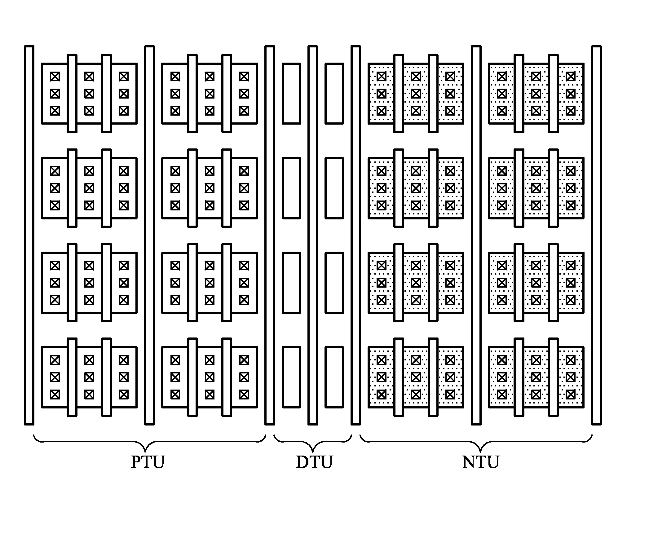
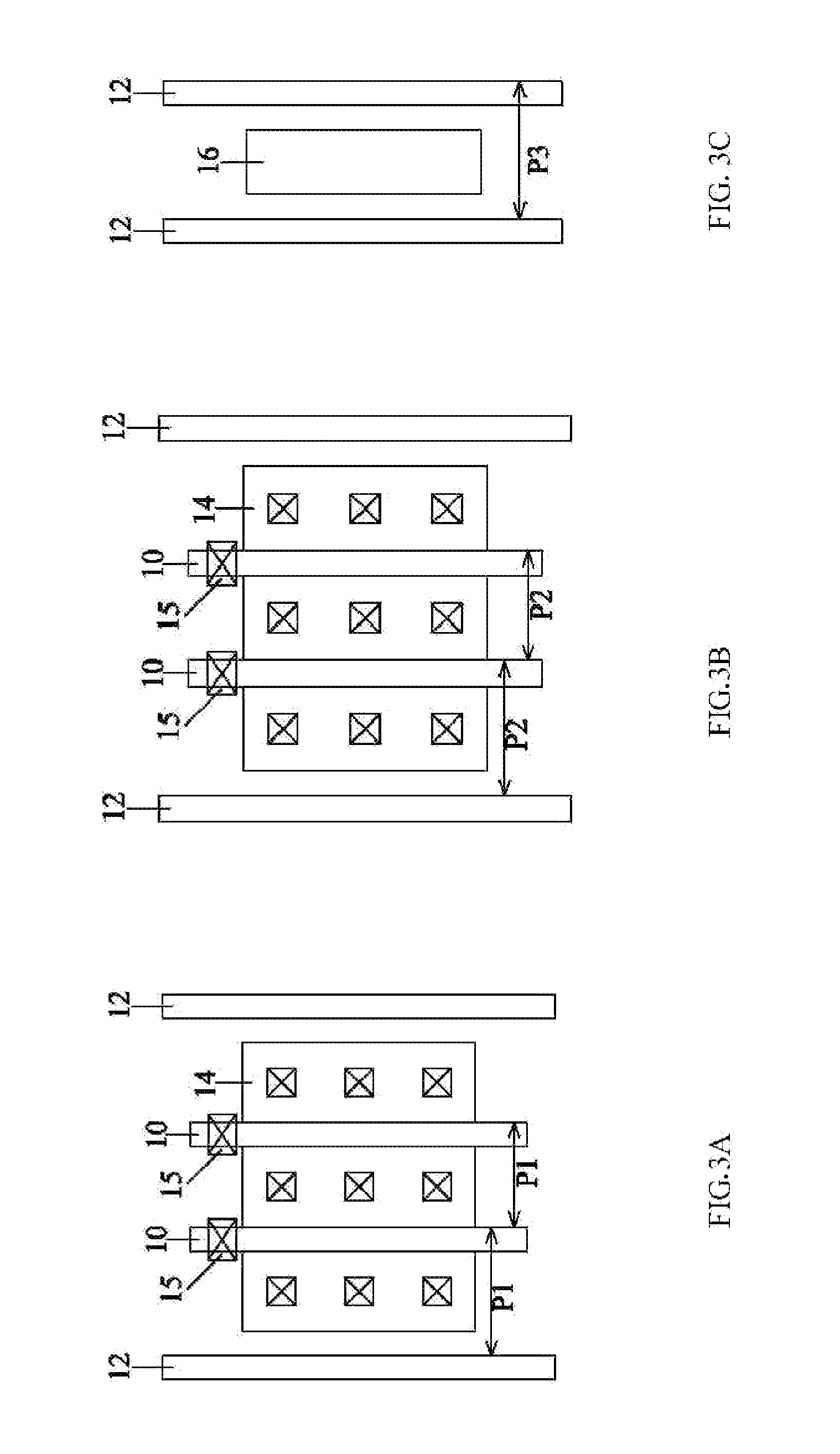
[0030]A novel method for developing integrated circuits is provided. Throughout the description, the term “Programmable Transistor Array” (PTA) is used to refer to array of Logic Transistor Units (LTUs) and / or arrays of Basic Transistor Units (BTUs), which may be interconnected (programmed) differently for different applications. The respective design methodology is referred to as a PTA methodology and the semiconductor chips manufactured using the PTA methodology (and hence including the LTUs) are accordingly referred to as PTA chips.

[0031]Each of the PTA chips includes a bas...


PUM


Abstract

A method of designing integrated circuits includes providing a first chip and a second chip identical to each other. Each of the first chip and the second chip includes a base layer including a Logic Transistor Unit (LTU) array. The LTU array includes LTUs identical to each other and arranged in rows and columns. The method further includes connecting the base layer of the first chip to form a first application chip; and connecting the base layer of the second chip to form a second application chip different from the first application chip.

Description

[0001]This application claims priority to U.S. Provisional Patent Application Ser. No. 61 / 146,564, filed Jan. 22, 2009, and entitled, “Programmable Transistor Array Design Methodology,” which application is hereby incorporated herein by reference.TECHNICAL FIELD[0002]This invention relates generally to integrated circuits and more particularly to the design methodology of integrated circuits.BACKGROUND[0003]The design of integrated circuits typically includes several phases. Before mass production of the integrated circuits, prototypes are typically made to verify the design of the integrated circuits. Field programmable gate array (FPGA) and cell based design (CBD) are among the most commonly used design methods.[0004]FIG. 1 illustrates a FPGA design, which includes a plurality logic units placed in an array, with predefined interconnects (not shown) built in. The FPGA may be programmed through an anti-fuse switch box (not shown), so that chips having a same FPGA design may be used...

Claims


Application Information

Patent Timeline
Patent Type & Authority Applications(United States)
IPC IPC(8): H01L27/088G06F17/50
CPCG06F17/5045G06F17/5054G06F17/5068H01L25/18H01L27/0207H01L2924/0002H01L27/11807H01L2924/00G06F30/34G06F30/39G06F30/30G06F30/347G06F30/343
Inventor LAW, OSCAR M. K.WU, KUO H.
Owner TAIWAN SEMICON MFG CO LTD
Why Eureka
Try Eureka