Imaging device, control method therefor, and camera

a technology of image sensor and control method, which is applied in the direction of radio frequency controlled devices, television system scanning details, television systems, etc., can solve the problems of wasteful space and difficulty in adopting shared type pixel circuits in the cmos image sensor, and achieve the effect of reducing vertical noise and shading

Inactive Publication Date: 2010-07-22
SONY CORP
View PDF6 Cites 9 Cited by
  • Summary
  • Abstract
  • Description
  • Claims
  • Application Information

AI Technical Summary

Benefits of technology

[0042]The embodiments of the invention can

Problems solved by technology

However, the CMOS image sensor 3a has the pixel circuits shifted row by row, producing wasteful space which stands in the way of improving the integration scale of pixel circuits.
Due to the layout-originated problem, it is difficult to adopt shared type pixel circuits in the CMOS image sensor 3a as shown in FIG. 16.
This difficulty arises because th

Method used


Image

  • Imaging device, control method therefor, and camera
  • Imaging device, control method therefor, and camera
  • Imaging device, control method therefor, and camera

Examples


first embodiment

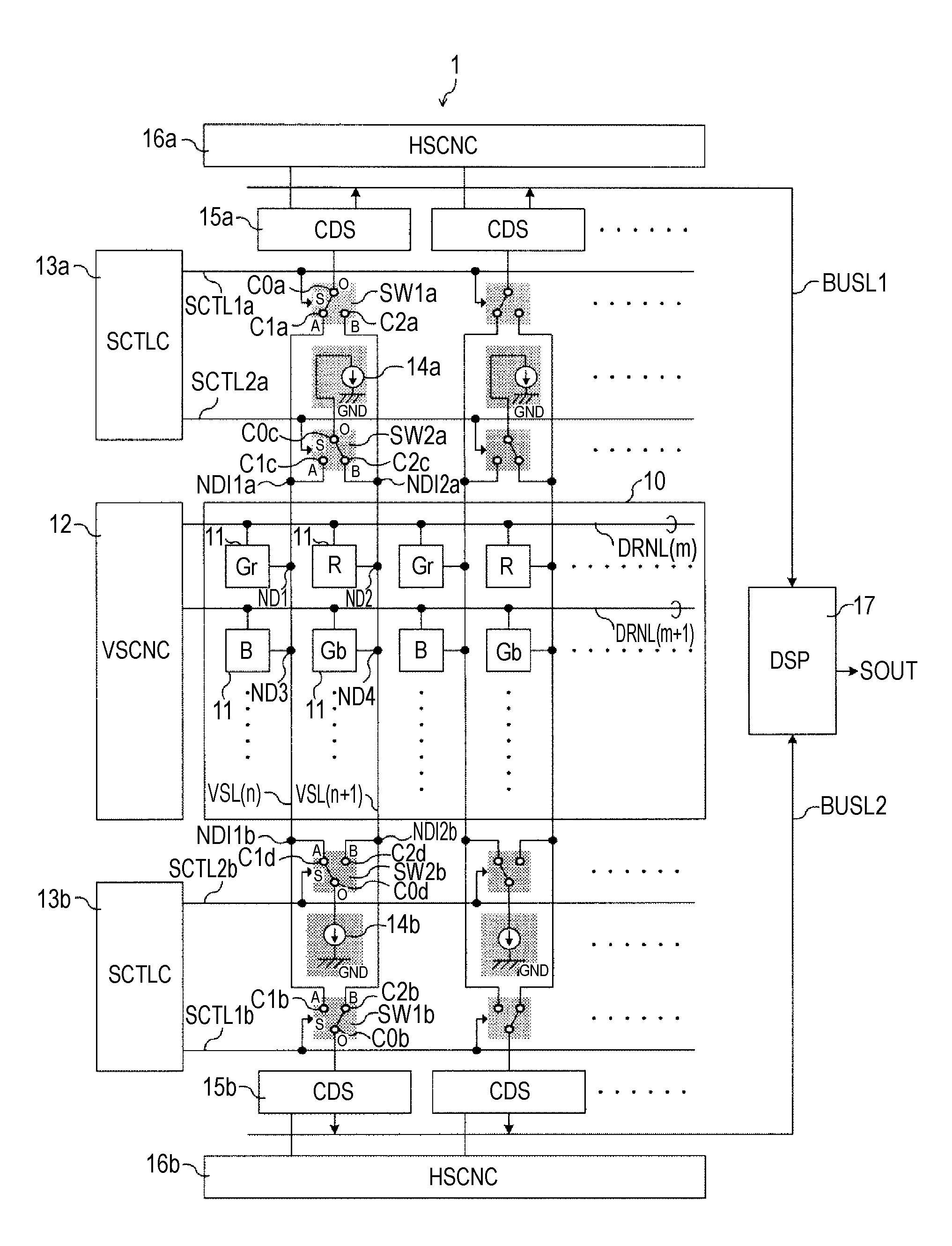
[0060]FIG. 1 is a schematic configurational diagram showing an example of the configuration of a CMOS image sensor according to a first embodiment.

[0061]As shown in FIG. 1, a CMOS image sensor (CMOS) 1 has a pixel section 10 and pixel circuits 11.

[0062]The CMOS image sensor 1 further has a row drive circuit (VSCNC) 12, selection control circuits (SCTLC) 13a, 13b, current sources 14a, 14b, CDS circuits (CDS) 15a, 15b, column drive circuits (HSCNC) 16a, 16b, and a data processing circuit (DSP) 17.

[0063]As shown in FIG. 1, the selection control circuit 13a, the current sources 14a, the CDS circuits 15a, the column drive circuit 16a, first path selection switches SW1a, and first current source selection switches SW2a are arranged on that side of the pixel section 10 where pixel circuits 11 in the first row are laid out (the side will be hereunder simply referred to as “upper stage”).

[0064]The selection control circuit 13b, the current sources 14b, the CDS circuits 15b, the column drive ...

second embodiment

[0171]A second embodiment will be described below. A CMOS image sensor according to the second embodiment uses the upper-stage selection control circuit 13a alone to control the first and second path selection switches SW1a, SW1b, and the first and second current source selection switches SW2a, SW2b. The following description will be given of only the differences from the first embodiment.

[0172]FIG. 8 is a schematic configurational diagram showing an example of the configuration of a CMOS image sensor la according to the second embodiment.

[0173]In the CMOS image sensor 1a, as shown in FIG. 8, the upper-stage selection control circuit 13a applies a selection signal S to the selection control line SCTL1a to control the first and second path selection switches SW1a, SW1b, and the first and second current source selection switches SW2a, SW2b.

[0174]Each switch is configured as shown in FIGS. 9A to 9C.

[0175]FIGS. 9A to 9C are diagrams for explaining the path selection switch and the curr...

third embodiment

[0201]A third embodiment will be described below. In a CMOS image sensor according to the third embodiment, four pixel circuits arranged in the column direction share a single output node.

[0202]FIG. 11 is a schematic configurational diagram showing an example of the configuration of a CMOS image sensor 1b according to the third embodiment.

[0203]As shown in FIG. 11, in a pixel section 10a of the CMOS image sensor 1b, four pixel circuits including Gr and B pixel circuits 11 in the nth column share a single node ND1, and four pixel circuits including R and Gb pixel circuits 11 in the (n+1)th column share a single node ND2. The pixel circuits with such a configuration are called “shared pixel circuits”.

[0204]Note that the four pixel circuits including Gr and B pixel circuits 11 in the nth column correspond to a first pixel circuit group according to the embodiment of the invention, and the four pixel circuits including R and Gb pixel circuits 11 in the (n+1)th column correspond to a sec...


PUM


Abstract

An imaging device includes: a pixel section having a plurality of pixel circuits arranged in a matrix form; and a signal processing section that processes an output signal read from the pixel section. The pixel section includes a first output signal line, at least one first color pixel circuit connected to the first output signal line, a second output signal line, and at least one second color pixel circuit adjacent to the first color pixel circuit in a row direction thereof and connected to the second output signal line. The signal processing section includes a first signal processing circuit, a second signal processing circuit, a selection circuit, a first current source, a second current source, a current source selection circuit, a first connection node, and a second connection node.

Description

BACKGROUND OF THE INVENTION[0001]1. Field of the Invention[0002]The present invention relates to an imaging device, such as a CMOS (Complementary Metal Oxide Semiconductor) image sensor, a control method therefor, and a camera.[0003]2. Description of the Related Art[0004]CMOS image sensors with various architectures to image a subject at a high speed have been proposed. For example, there is a CMOS image sensor which has an A / D converter provided for a column circuit to achieve faster imaging and lower noise (see JP-A-2005-278135 (Patent Document 1), for example).[0005]When the pitch between pixel circuits becomes narrower with an improved scale of the integration of the pixel circuits, it is difficult to install a plurality of CDS circuits in one column (one stage). There is a CMOS image sensor which achieves integration of pixel circuits by arranging a plurality of CDS circuits separated in upper and lower stages of a pixel section and allowing two systems of CDS circuits to proce...

Claims


Application Information

Patent Timeline
IPC IPC(8): H04N5/335H01L27/146H04N5/341H04N5/357H04N5/361H04N5/363H04N5/369H04N5/374H04N5/3745H04N5/378H04N9/07
CPCH01L27/14645H04N5/3658H04N5/3742H04N5/3745H04N9/045H04N25/677H04N25/767H04N25/77
Inventor YAMAGATA, YUUKIKOSEKI, KEN
Owner SONY CORP
Why Eureka
Try Eureka