Substrates Having Voltage Switchable Dielectric Materials

Inactive Publication Date: 2010-07-29
LITTELFUSE INC
View PDF55 Cites 21 Cited by
  • Summary
  • Abstract
  • Description
  • Claims
  • Application Information

AI Technical Summary

Benefits of technology

[0016]Various aspects provide for the incorporation of a voltage switchable dielectric material into a substrate in a manner that results in the substrate meeting various specifications, including dimensionality specifications. In some embodiments, a method for designing a PCB to meet a specification may comprise choosing a first design for a PCB comprising one or more prepreg layers. A first r

Problems solved by technology

In some cases, a substrate may be inadvertently deformed during processing (e.g., during curing of a PCB).
Processing a VSDM layer on a PCB may cause warping, which may be undesirable.
In some cases, imbalance may not be manifest until subsequent processing (e.g., curing the PC

Method used


Image

  • Substrates Having Voltage Switchable Dielectric Materials
  • Substrates Having Voltage Switchable Dielectric Materials
  • Substrates Having Voltage Switchable Dielectric Materials

Examples


Embodiment Construction

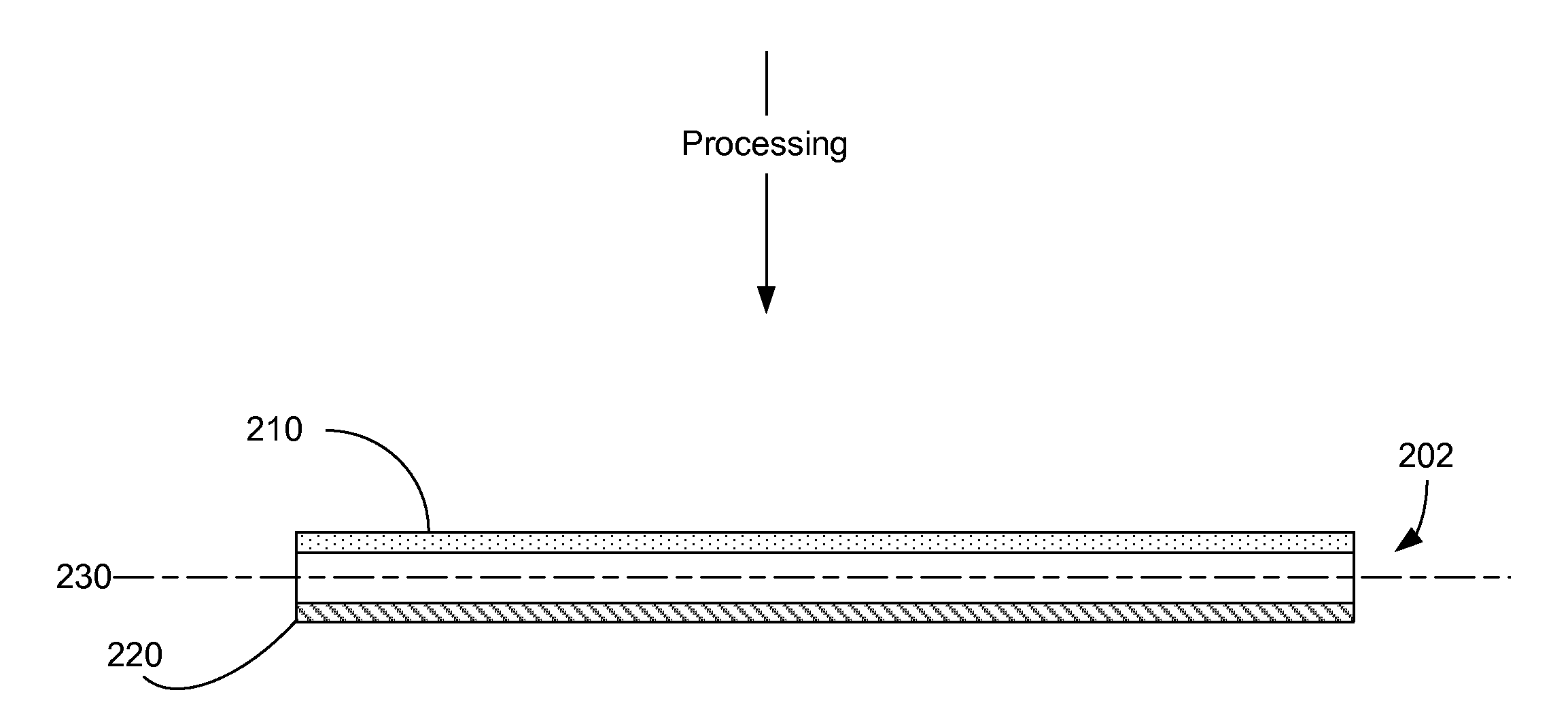
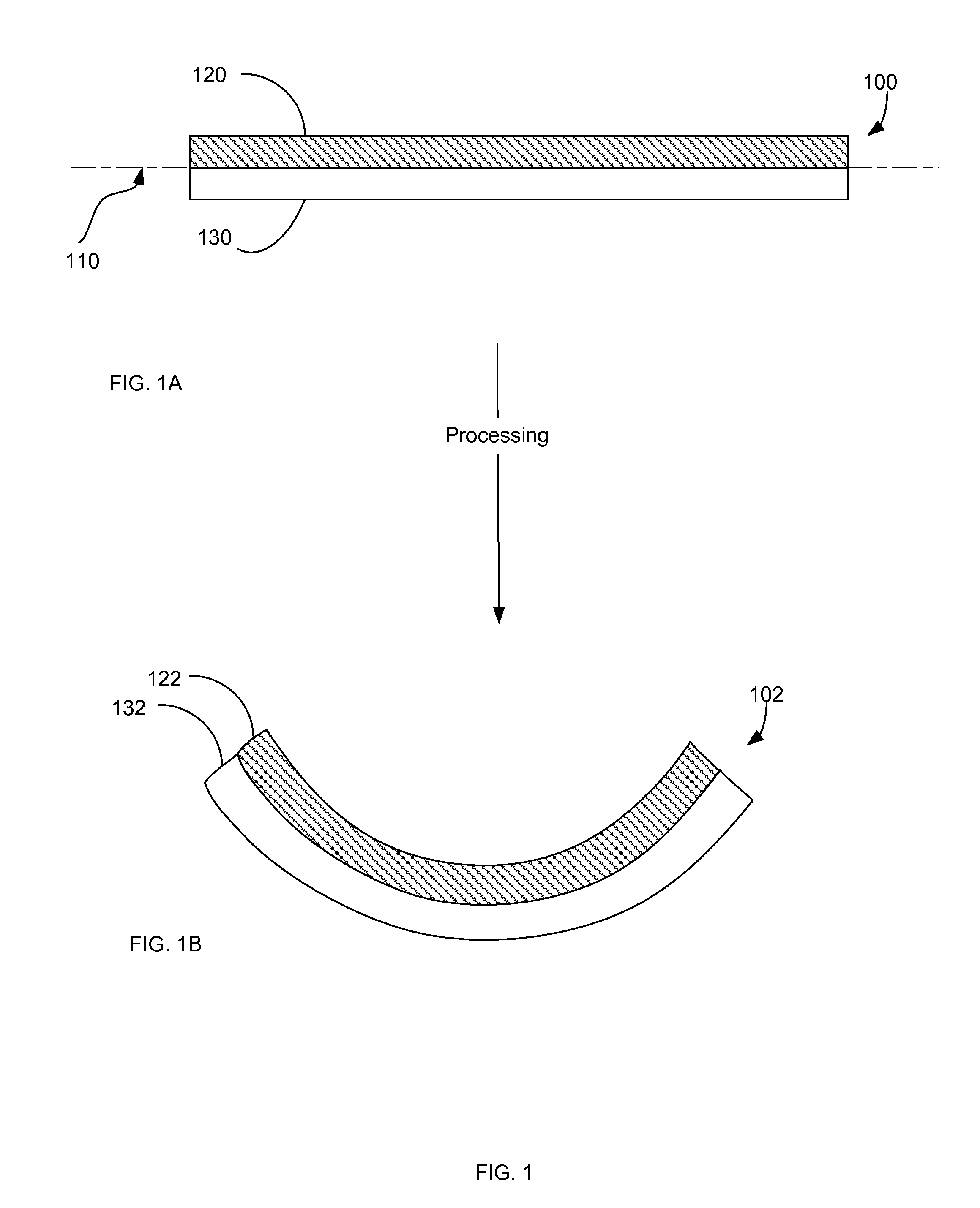
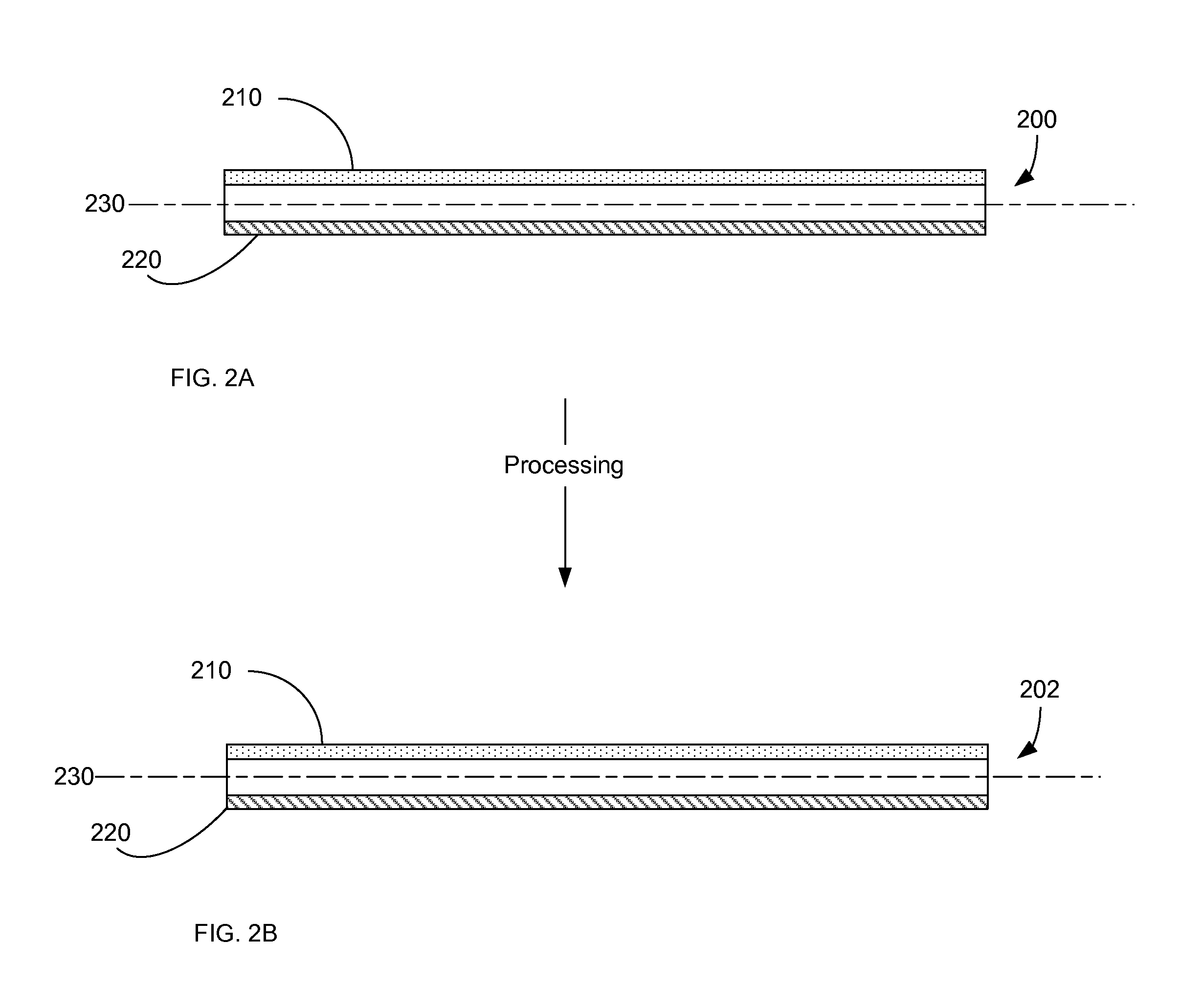
[0033]Various aspects provide for incorporating a VSDM into a substrate to create an ESD-protected substrate. In some cases, a VSDM is incorporated in a manner that results in the ESD-protected substrate meeting one or more specifications (e.g., thickness, planarity, and the like) for various subsequent processes or applications. Various aspects provide for designing a substrate (e.g., a PCB) incorporating a VSDM, and adjusting one or more aspects of the substrate to design a balanced, ESD-protected substrate. Certain embodiments include an ESD-protected substrate (e.g., incorporating a VSDM) that is mechanically and / or elastically balanced, but may not display a structural symmetry (e.g., mirror symmetry) with respect to a centerline through the substrate.

[0034]In some embodiments, a specification for a PCB is received, a VSDM is incorporated, and a balance region is incorporated into the design of the PCB to accommodate the incorporation of the VSDM while meeting the specification...


PUM

PropertyMeasurementUnit
Fractionaaaaaaaaaa
Angleaaaaaaaaaa
Shrinkageaaaaaaaaaa

Abstract

Various aspects provide for incorporating a VSDM into a substrate to create an ESD-protected substrate. In some cases, a VSDM is incorporated in a manner that results in the ESD-protected substrate meeting one or more specifications (e.g., thickness, planarity, and the like) for various subsequent processes or applications. Various aspects provide for designing a substrate (e.g., a PCB) incorporating a VSDM, and adjusting one or more aspects of the substrate to design a balanced, ESD-protected substrate. Certain embodiments include molding a substrate having a VSDM layer into a first shape.

Description

CROSS REFERENCE TO RELATED APPLICATIONS[0001]This application claims the priority benefit of U.S. provisional patent application No. 61 / 147,730, filed Jan. 27, 2009 and entitled “Techniques for Reducing Warpage in the Application of VSD Material to Core and Substrate,” which is incorporated by reference herein.BACKGROUND[0002]1. Technical Field[0003]The present invention relates to designing and fabricating objects that incorporate voltage switchable dielectric materials.[0004]2. Description of Related Art[0005]A printed circuit board, printed wiring board, integrated circuit (IC) package, or similar substrate (hereinafter, PCB) may be used to assemble and connect electronic components. A PCB typically includes a dielectric material and one or more conductive leads to provide electrical conductivity among various attached components, chips, and the like. In some cases, metallic leads may be included (e.g., as a layer of Cu which is subsequently etched) to provide electrical connecti...

Claims


Application Information

Patent Timeline
IPC IPC(8): H05K9/00G06F17/50B05D5/12
CPCH05K1/0259H05K1/0271H05K1/036H05K1/0373H05K3/0005H05K2201/068H05K2201/0738H05K2201/09136Y10T428/24917Y10T428/24942
Inventor KOSOWSKY, LEXGRAYDON, BHRETMOUSTAFAEV, DJABBARSHANG, SHURUIFLEMING, ROBERT
Owner LITTELFUSE INC
Why Eureka
Try Eureka