

Isolated switching power supply device
a power supply device and isolation technology, applied in the direction of electric variable regulation, process and machine control, instruments, etc., can solve the problems of large size, high cost, and inability to meet the requirements of relatively high power, and achieve the reduction of size and cost of the resulting device, high circuit efficiency, and high power capacity
- Summary
- Abstract
- Description
- Claims
- Application Information
AI Technical Summary
Benefits of technology
Problems solved by technology
Method used
Image

Examples
first preferred embodiment
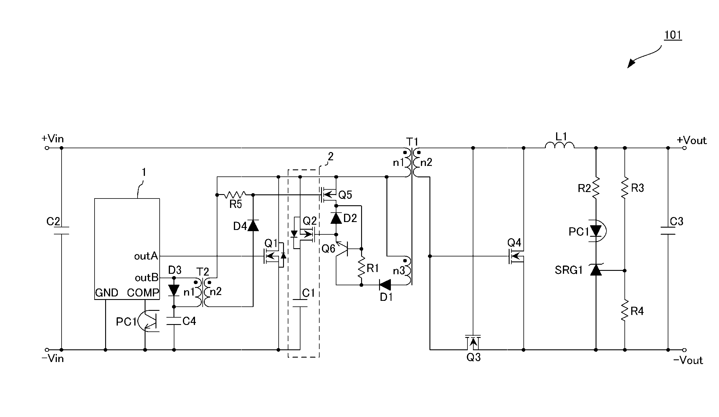
[0048]FIG. 5 is a circuit diagram of an isolated switching power supply device 101 according to a first preferred embodiment of the present invention. FIG. 6 shows waveforms of some portions of the isolated switching power supply device 101, and FIGS. 7A-7D show the structure of a multiple transformer used in the isolated switching power supply device 101.
[0049]In FIG. 5, the isolated switching power supply 101 includes a main transformer T1. A series circuit including a clamp capacitor C1 and a clamp switch Q2 is connected to the primary coil n1 of the main transformer T in series to define a voltage clamping circuit 2. The clamp switch Q2 preferably is an n-type channel MOSFET, and has a parasitic diode in parallel. A switching control circuit 1 is a PWM (pulse width modulation) control IC that drives the active clamp converter or the isolated power supply device 101. The switching control circuit 1 includes a power switch driving terminal outA, a clamp switch driving terminal out...
second preferred embodiment
[0075]FIG. 8 is a circuit diagram of an isolated switching power supply device 102 according to a second preferred embodiment of the present invention. FIG. 9 shows waveforms of some portions of the isolated switching power supply device 102.
[0076]Subsequently, the same configuration as that in the first preferred embodiment shown in FIG. 5 is provided on the primary side of the main transformer T1. On the secondary side of the main transformer T1 are disposed a rectifying diode D5, an output smoothing capacitor C3, resistors R2, R3 and R4, an ELD of the photo coupler PC1, and a shunt regulator SRG1.
[0077]The isolated switching power supply device 102 of the second preferred embodiment acts as an active clamp flyback converter. The configuration of the clamp switch driving circuit and the feedback operation of output voltages are the same as in the first preferred embodiment, and how the power is converted will now be described.
[0078]A DC voltage applied between the terminals +Vin a...
third preferred embodiment
[0083]FIG. 10 is a circuit diagram of an isolated switching power supply device 103 according to a third preferred embodiment of the present invention. FIG. 11 shows waveforms of some portions of the isolated switching power supply device 103. The isolated switching power supply device 103 of the third preferred embodiment acts as an asymmetrical control half bridge converter. The asymmetrical control refers to a controlling technique for controlling the driving of the power switch Q1 and the clamp switch Q2 with complementary timing with dead time periods for which both switches are off. Thus, PWM control is performed such that when the pulse width of the power switch Q1 is increased, the pulse width of the clamp switch Q2 is reduced, and when the pulse width of the power switch Q1 is reduced, the pulse width of the clamp switch Q2 is increased. As shown in FIG. 11, the waveform in operation is similar to that of the active clamp flyback converter of the second preferred embodiment...
PUM
 Abstract
Description
Claims
Application Information