High-linearity broadband stacking low noise amplifier based on gain compensation technology

A low-noise amplifier and low-noise amplification technology, which is applied in field-effect transistor RF low-noise amplifiers and integrated circuits, can solve the problems of increasing chip cost, low amplifier power consumption, large chip area, etc., achieve good input and output matching, and facilitate gain Compression compensation, the effect of improving the linearity index

Active Publication Date: 2017-11-07
CHENGDU GANIDE TECH
View PDF5 Cites 23 Cited by
  • Summary
  • Abstract
  • Description
  • Claims
  • Application Information

AI Technical Summary

Problems solved by technology

[0004] (1) Low power consumption, high gain, and low noise amplification indicators mutually restrict each other: driven by the market, the standby power consumption of the RF front-end receiver needs to be reduced as much as possible, so as to realize the function of energy saving, but the traditional common source (or common emitter) In the design of low-noise amplifiers, the best noise bias point to achieve optimal noise and the bias point to meet the maximum gain and transconductance often cannot achieve the lowest power consumption of the amplifier, so the two indicators are not well compatible.
[0005] (2) Low power consumption and high linearity index mutually restrict each other: in traditional common-source (or common-emitter) low-noise amplifier design, high linearity index needs to select amplifier transistors with high power capacity and high 1dB compression point under a fixed process, However, high power capacity often requires large DC

Method used


Image

  • High-linearity broadband stacking low noise amplifier based on gain compensation technology
  • High-linearity broadband stacking low noise amplifier based on gain compensation technology

Examples


Embodiment Construction

[0032] The principles and features of the present invention are described below in conjunction with the accompanying drawings, and the examples given are only used to explain the present invention, and are not intended to limit the scope of the present invention.

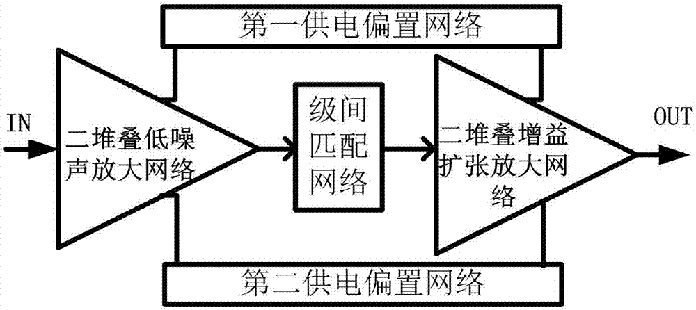
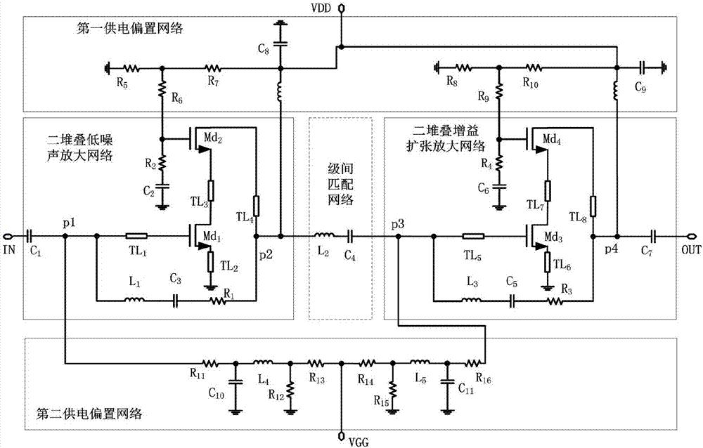
[0033] like figure 1 , figure 2 As shown, the present invention provides a high-linearity broadband stacked low-noise amplifier based on gain compensation technology, which is an ultra-wideband high-linearity stacked low-noise amplifier with two stacked low-noise amplifying networks and two-stacked gain expansion amplifying networks as the core Amplifiers, designed using integrated circuit technology.

[0034] The low noise amplifier includes two stacked low noise amplifying networks, an interstage matching network and two stacking gain expansion amplifying networks connected in sequence; and the first power supply connected to the two stacking low noise amplifying networks and the two stacking gain expanding ampl...


PUM


Abstract

The invention discloses a high-linearity broadband stacking low noise amplifier based on a gain compensation technology. The high-linearity broadband stacking low noise amplifier comprises a two-stacking low noise amplification network, an interstage matching network and a two-stacking gain expansion amplification network which are connected in sequence; and a first power supply bias network and a second power supply bias network which are connected with the two-stacking low noise amplification network and the two-stacking gain expansion amplification network. According to the high-linearity broadband stacking low noise amplifier, a serial stacking structure is realized through adoption of two transistors with different sizes and ultra wide band noise and impedance matching are realized through combination of an RLC feedback network; through utilization of the gain compression compensation technology, the gain compression property of the two-stacking low noise amplification network is cancelled within a certain bias range through the two-stacking gain expansion amplification network and a linearity index of the amplifier is improved, so the whole low noise amplifier has good broadband, linearity, low power consumption and low noise amplification capability; and moreover, the low breakdown voltage property of an integrated circuit technology is avoided and the stability and reliability of a circuit are improved.

Description

technical field [0001] The invention relates to the fields of field effect transistor radio frequency low noise amplifiers and integrated circuits, in particular to a high linearity, wideband, low power consumption low noise amplifier applied to a receiving module at the front end of an ultra-wideband receiver. Background technique [0002] With the rapid development of electronic warfare, software radio, ultra-wideband communication, wireless local area network (WLAN) and other military electronic warfare and communication, and civilian communication markets, RF front-end receivers are also developing in the direction of high performance, high integration, and low power consumption. Therefore, the market urgently needs ultra-wideband, high gain, high linearity, low power consumption, and low noise RF and microwave low noise amplifier chips. [0003] However, when designing traditional radio frequency and microwave low noise amplifier chips, there are always some design prob...

Claims


Application Information

Patent Timeline
IPC IPC(8): H03F1/02H03F1/26H03F1/32H03F1/48H03F1/56H03F3/193
CPCH03F1/0216H03F1/26H03F1/3205H03F1/483H03F1/56H03F3/193H03F2200/318H03F2200/294H03F2200/451Y02D30/70
Inventor 吕继平邬海峰滑育楠陈依军廖学介胡柳林童伟王测天
Owner CHENGDU GANIDE TECH
Why Eureka
Try Eureka