Semiconductor Wafer Carrier

Active Publication Date: 2010-08-05
TAIWAN SEMICON MFG CO LTD
View PDF43 Cites 13 Cited by
  • Summary
  • Abstract
  • Description
  • Claims
  • Application Information

AI Technical Summary

Benefits of technology

[0010]An advantage of a preferred embodiment of the present invention is the protection of a semicond

Problems solved by technology

Generally, semiconductor wafers can be thin and vulnerable to damage, and can become even thinner and more vulnerable to damage during processing.
This process of thinning the wafer can damage the edges of the wafer and can make the wafer even more fragile and susceptible to damage during subsequent transportation and processing of the wafer.
However, by attaching the waf

Method used


Image

  • Semiconductor Wafer Carrier
  • Semiconductor Wafer Carrier
  • Semiconductor Wafer Carrier

Examples


Embodiment Construction

[0019]The making and using of the presently preferred embodiments are discussed in detail below. It should be appreciated, however, that the present invention provides many applicable inventive concepts that can be embodied in a wide variety of specific contexts. The specific embodiments discussed are merely illustrative of specific ways to make and use the invention, and do not limit the scope of the invention.

[0020]The present invention will be described with respect to preferred embodiments in a specific context, namely a process of attaching a semiconductor wafer to a carrier during a thinning process to expose through silicon vias (TSV). The invention may also be applied, however, to other processes in which it may be beneficial to utilize a carrier substrate.

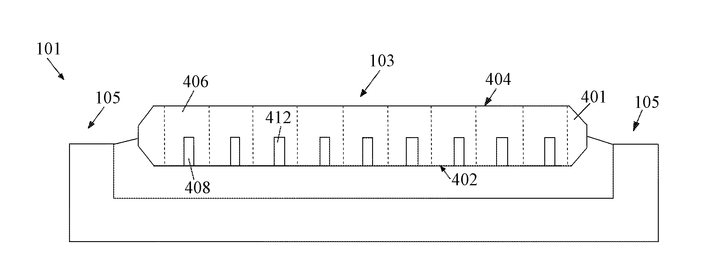
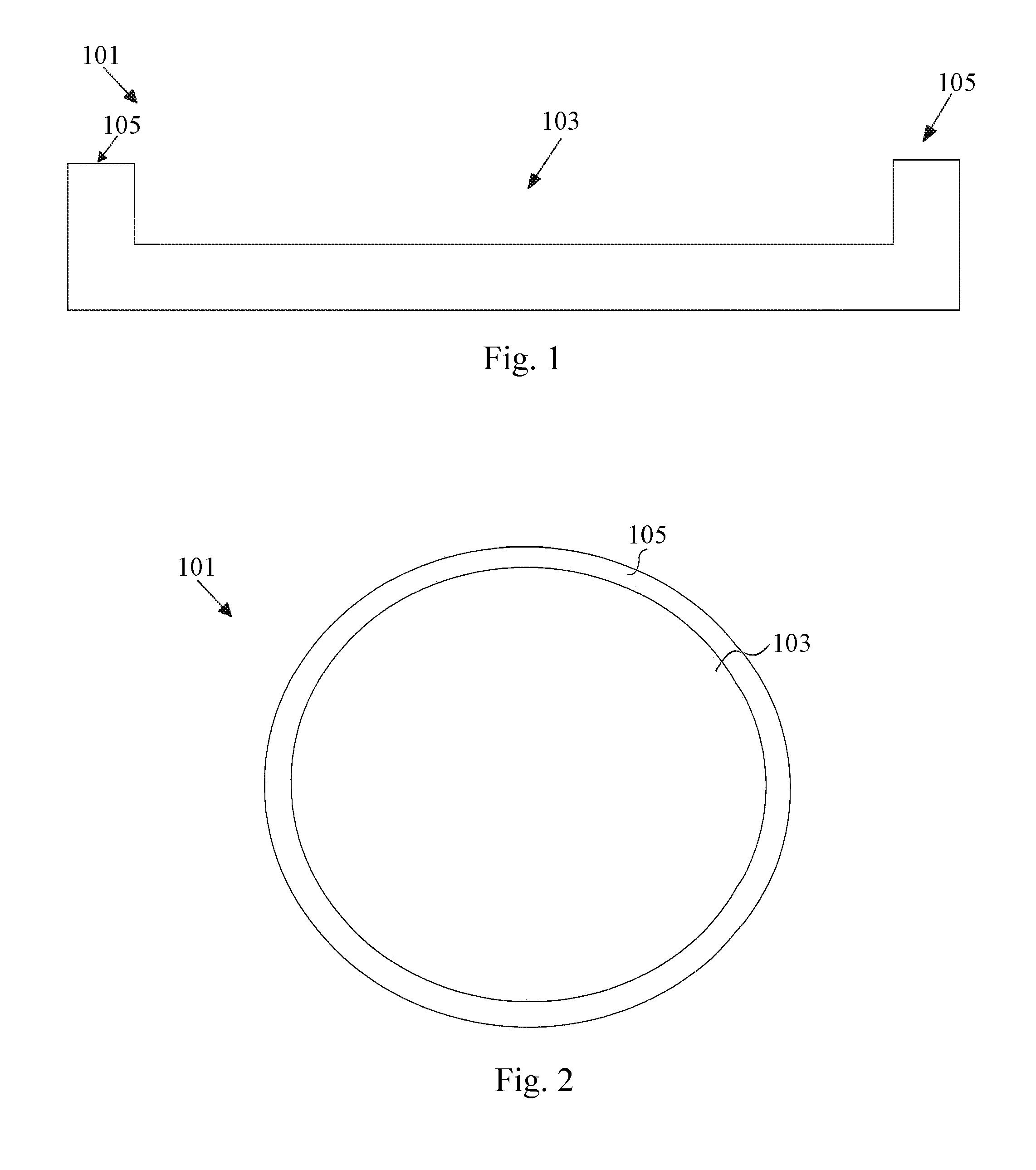
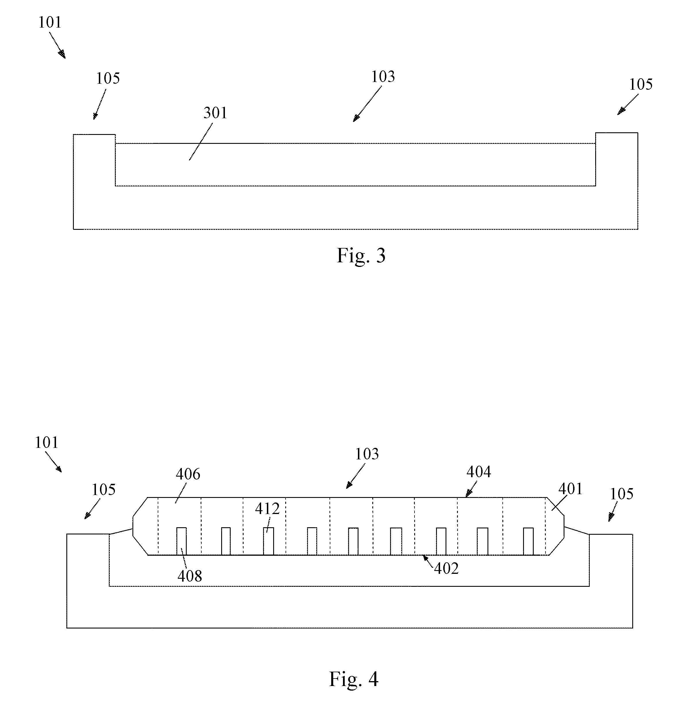
[0021]With reference now to FIG. 1, there is shown a cross-sectional view of a preferred carrier 101. The carrier 101 preferably comprises, for example, glass, silicon oxide, aluminum oxide, combinations of these, or the l...


PUM

PropertyMeasurementUnit
Lengthaaaaaaaaaa
Lengthaaaaaaaaaa
Thicknessaaaaaaaaaa

Abstract

A system and a method for protecting semiconductor wafers is disclosed. A preferred embodiment comprises a carrier with a central region and an exterior region. The exterior region preferably has a thickness that is greater than the central region, to form a cavity in the carrier. An adhesive is preferably placed into the cavity, and a semiconductor wafer is placed onto the adhesive. The edges of the semiconductor wafer are protected by the raised exterior region as well as the displaced adhesive that at least partially fills the area between the semiconductor wafer and the exterior region of the carrier.

Description

[0001]This application claims the benefit of U.S. Provisional Patent Application Ser. No. 61 / 149,206, filed on Feb. 2, 2009, and entitled “Semiconductor Wafer Carrier,” which application is incorporated herein by reference.TECHNICAL FIELD[0002]The present invention relates generally to a system and a method for manufacturing semiconductor devices and, more particularly, to a system and method for carrying semiconductor wafers.BACKGROUND[0003]Generally, semiconductor wafers can be thin and vulnerable to damage, and can become even thinner and more vulnerable to damage during processing. One such step that can make the semiconductor wafer thinner is a through silicon via (TSV) process, whereby conductive vias are formed in a front side of the wafer and the backside of the wafer is thinned through a process such as grinding in order to expose the conductive vias from the backside. This process of thinning the wafer can damage the edges of the wafer and can make the wafer even more frag...

Claims


Application Information

Patent Timeline
IPC IPC(8): H01L21/673B29C65/14
CPCH01L21/67346Y10T29/53961H01L21/67132Y10T29/4913
Inventor HUANG, JAO SHENGCHEN, MING-FA
Owner TAIWAN SEMICON MFG CO LTD
Why Eureka
Try Eureka