
ROM array

a rom array and array technology, applied in the field of rom arrays, can solve the problems of significant leakage across the memory cells, significant slowdown of the switching speed of the line, and can consume around 25% of the cycle, and achieve the effects of improving the density of the rom array, and reducing the cost of rom arrays

Active Publication Date: 2010-08-05
ARM LTD
View PDF5 Cites 3 Cited by
  • Summary
  • Abstract
  • Description
  • Claims
  • Application Information

AI Technical Summary

Benefits of technology

[0009]The inventors of the present invention found that an advantageous degree of ROM array density improvement could be achieved by providing plural columns of memory cells, wherein each column of memory cells is coupled to a shared bit line, the shared bit line being shared by one column of memory cells with an adjacent column of memory cells. Advantageously only a relatively simple arrangement of readout circuitry is then found to be necessary if those columns of memory cells is connected to its own associated reference line. Furthermore, it has been found that sharing reference lines between columns of memory cells provides a rather limited space saving benefit and this minor advantage is often outweighed by the high capacitive load of a shared reference line, which may significantly slow down the switching speed of that line.
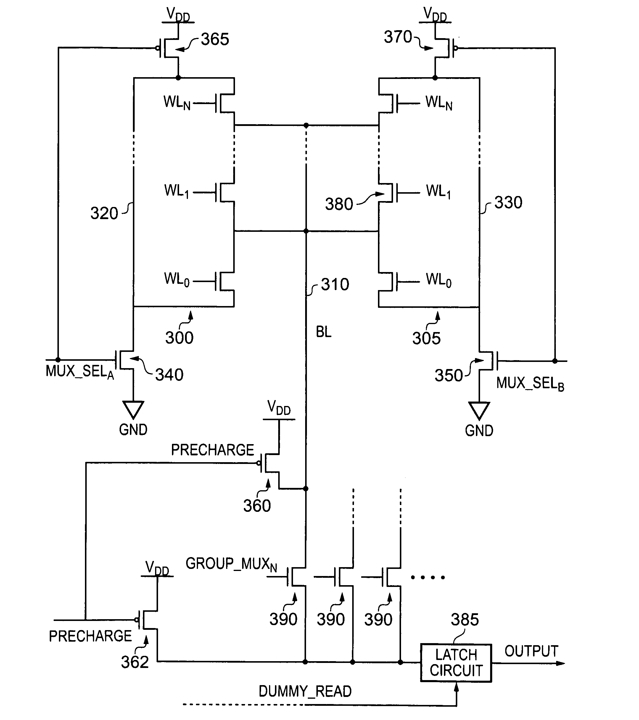
[0010]Furthermore, by associating switch circuitry with each reference line, wherein that switch circuitry is arranged to selectively couple that reference line to a reference potential, at least two advantages result.
[0011]Firstly, the pre-charging of each (shared) bit line can take place earlier in the read cycle, since by decoupling from the reference potential both of the reference lines associated with the two columns of memory cells that share a bit line, that bit line can be pre-charged without significant leakage occurring in those memory cells. Hence, the bit line may be pre-charged prior to the read cycle commencing. Without being able to decouple the reference lines from the reference potential, pre-charging the bit line prior to the read cycle in this manner would lead to significant leakage across the memory cells. Thus, according to the techniques of the present invention, not only is leakage reduced, but reading speed is also increased because the bit line is already pre-charged at the start of the read cycle and a delay whilst pre-charging the bit line during the read cycle is avoided. This pre-charging delay can consume around 25% of the cycle.
[0014]In one embodiment, each reference line has further associated switch circuitry arranged to selectively couple that reference line to an alternative potential different to said reference potential, each reference line being connected to said alternative potential by said further associated switch circuitry when that reference line is not connected to said reference potential. By connecting each reference line to the alternative potential when that reference line is not connected to the reference potential, and hence when the corresponding column of memory cells is not being read, the opportunity for that reference line to float at an unknown voltage level is avoided, which could otherwise lead to charge sharing across the column of memory cells that is not being read, and hence read errors on the shared bit line. In this embodiment it may be arranged that the further associated switch circuitry couples its associated reference line to said alternative potential when said column selection signal is not asserted. Hence the column selection signal provides the determination both for when to connect each reference line to the reference potential and also (anti-correlated thereto) when to connect each reference line to the alternative potential.
[0017]In one embodiment, at least one column of said plurality of columns of memory cells is a dummy column for self-timing of the read operation. Self-timing of the read operation is a convenient method of reliably timing the read operation and a dummy column of memory cells, arranged for the purpose of providing timing information, provides a useful source of this information at the minor cost of a column of memory cells in which regular data is not stored. According to this embodiment, it may be arranged that said dummy column generates a dummy read signal for said self-timing of the read operation. This dummy read signal may then be conveniently passed to whichever locations in the ROM array it is required for self-timing purposes.
[0019]In one embodiment a data value readout from said shared bit line is stored in a latch circuit. By storing the data value in a latch circuit, that data value is then temporarily saved, and the shared bit line is then freed up to be pre-charged ready for a subsequent read. The data value stored in the latch circuit can then be read out when needed. In this embodiment it may be arranged that a plurality of shared bit lines share said latch circuit, each of said plurality of shared bit lines being coupled to said latch circuit by shared bit line switch circuitry in dependence on a shared bit line selection signal. Space and power saving advantages may be derived from the arrangement of multiple shared bit lines being coupled to one latch circuit, and the selection of which shared bit line should be connected at any given time to the latch circuit is conveniently provided by a shared bit line selection signal.

Problems solved by technology

Furthermore, it has been found that sharing reference lines between columns of memory cells provides a rather limited space saving benefit and this minor advantage is often outweighed by the high capacitive load of a shared reference line, which may significantly slow down the switching speed of that line.
Without being able to decouple the reference lines from the reference potential, pre-charging the bit line prior to the read cycle in this manner would lead to significant leakage across the memory cells.
This pre-charging delay can consume around 25% of the cycle.

Method used


Image

  • ROM array
  • ROM array
  • ROM array

Examples


Embodiment Construction

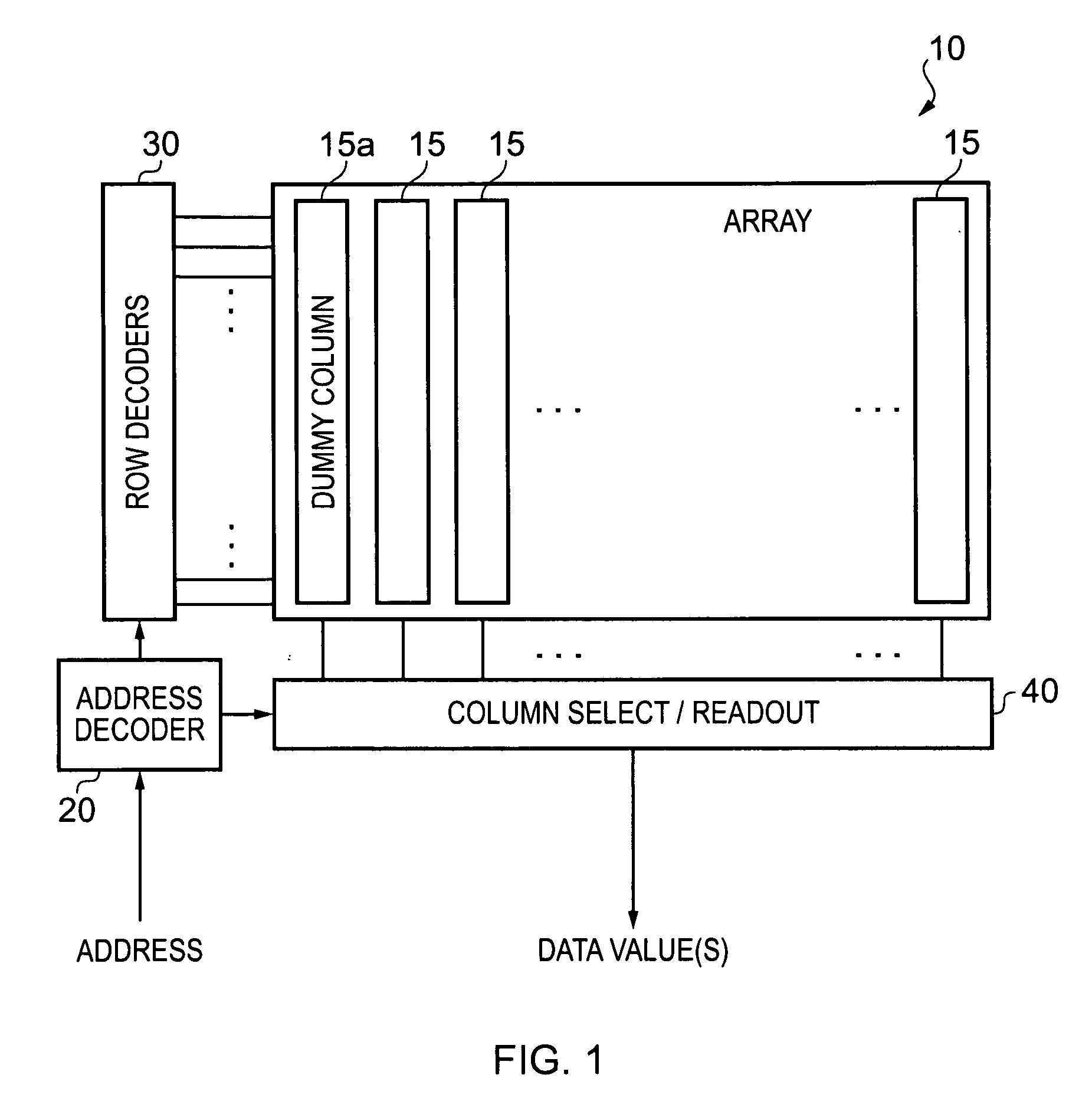
[0029]FIG. 1 schematically illustrates a ROM array according to one embodiment of the present invention. ROM array 10 comprises columns of memory cells 15 arranged in an array. Data stored in the memory cells of the ROM array is accessed by means of an address received by address decoder 20. Address decoder 20 passes control signals to row decoders 30 and column select / readout circuitry 40. A data value stored in a particular memory cell at the intersection of a given row and column is then read out, the data value being passed via column select / readout circuitry 40. The columns of memory cells 15 include a dummy column 15A which is not used to store data values for reading out, but rather to produce timing information for self-timing a read operation on one of the other columns.

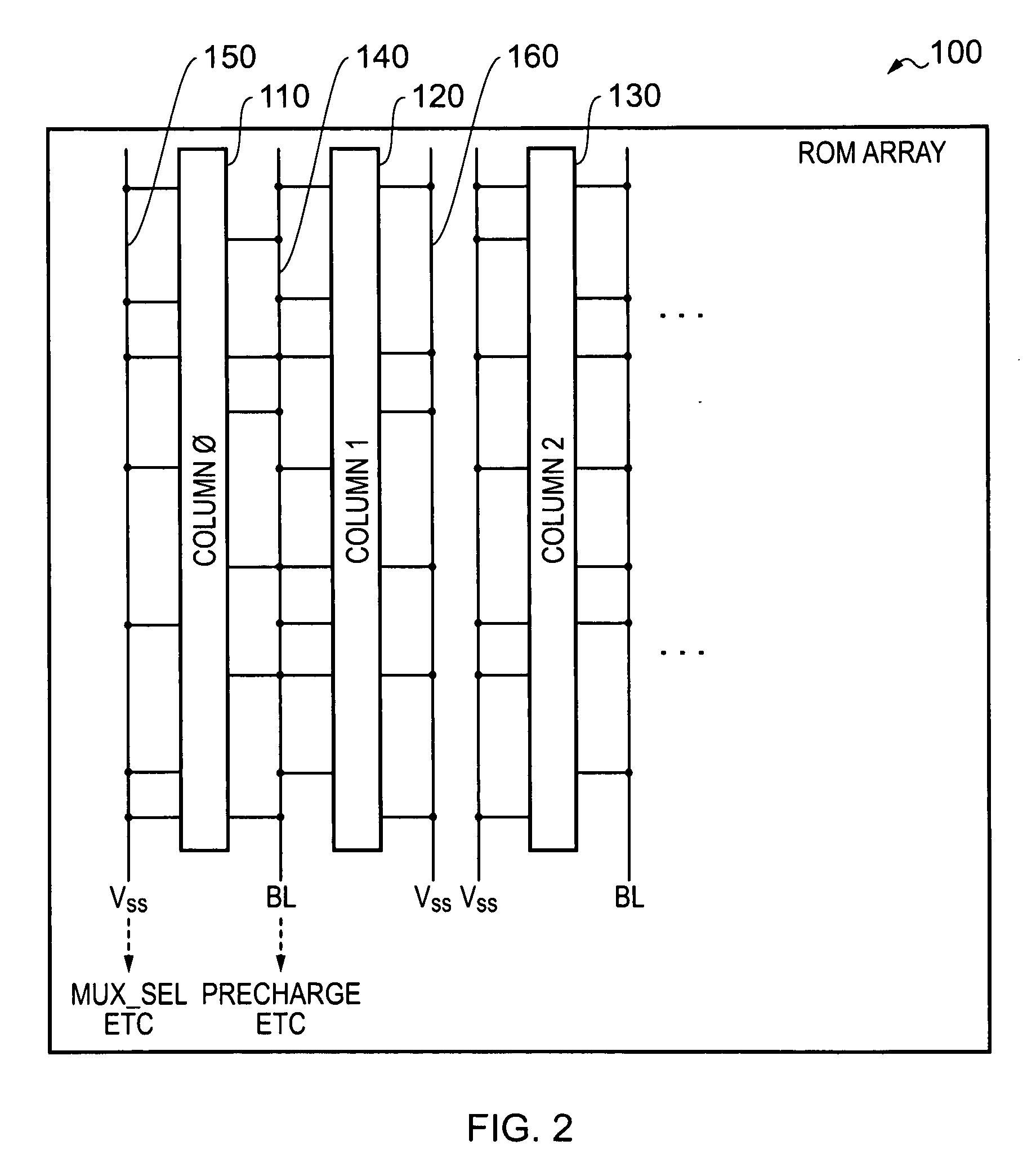
[0030]Further detail of a ROM array according to one embodiment of the present invention is schematically illustrated in FIG. 2. As in FIG. 1, the ROM array 100 comprises a plurality of columns of memory cel...


PUM


Abstract

A ROM array is provided, comprising a plurality of columns of memory cells, wherein each column of memory cells is coupled to a shared bit line which is shared by that column of memory cells and an adjacent column of memory cells. Each column of memory cells has its own associated reference line, which is selectively coupled to a reference potential. Each reference line is coupled to the reference potential when a read operation is performed on a memory cell of the associated column of memory cells. Each reference line is decoupled from the reference potential when a read operation is performed on a memory cell of the adjacent column of memory cells. Both reference lines associated, via their columns of memory cells, to a shared bit line are decoupled from the reference potential when the shared bit line is being pre-charged prior to the read operation. The present invention thus provides a ROM array in which both leakage reduction and speed increase benefits result, whilst providing a high density design.

Description

BACKGROUND OF THE INVENTION[0001]1. Field of the Invention[0002]The present invention relates to ROM arrays.[0003]2. Description of the Prior Art[0004]ROM arrays composed of columns and rows of memory cells are known in the art. When a data value is required to be read out from such a ROM array, first the row of memory cells containing the memory cell holding the required data value is selected by activating a word line corresponding to that row. Then a bit line associated with the column of memory cells containing the memory cell holding the required data value is used to perform a read operation on the value stored in the selected memory cell. Typically this read operation is carried out by pre-charging the selected bit line and then measuring the discharge that occurs when the relevant memory cell is activated by means of its corresponding word line.[0005]Various techniques have been proposed to achieve high density ROM arrays. In U.S. Pat. No. 5,917,224 a compact ROM matrix is d...

Claims


Application Information

Patent Timeline
Patent Type & Authority Applications(United States)
IPC IPC(8): G11C17/00G11C7/00
CPCG11C7/12G11C7/14G11C2207/2281G11C7/22G11C7/18
Inventor THYAGARAJAN, SRIRAMYEUNG, GUSSOWDEN, ANDREW JOHN
Owner ARM LTD
Learn More