Package structure for wireless communication module

a wireless communication module and packaging technology, applied in the direction of electrical equipment, semiconductor devices, semiconductor/solid-state device details, etc., can solve the problem of lowering and achieve the effect of increasing the yield of the emi shielding test and increasing the peak

Active Publication Date: 2010-08-12
ADVANCED SEMICON ENG INC
View PDF4 Cites 13 Cited by
  • Summary
  • Abstract
  • Description
  • Claims
  • Application Information

AI Technical Summary

Benefits of technology

[0007]A primary object of the present invention is to provide a package structure for a wireless communication module, wherein an upper surface of a substrate has an annular ground pad, a supporting region defined within the annular ground pad, and an auxiliary ground pad in the supporting region, while a shielding lid has an auxiliary ground portio

Problems solved by technology

However, the technical problem of the traditional package structure of the wireless communication module is described as follows: although the shielding lid 15 can restrict the electromagnetic waves generated by the chip 12 therein to prevent from

Method used


Image

  • Package structure for wireless communication module
  • Package structure for wireless communication module
  • Package structure for wireless communication module

Examples


Embodiment Construction

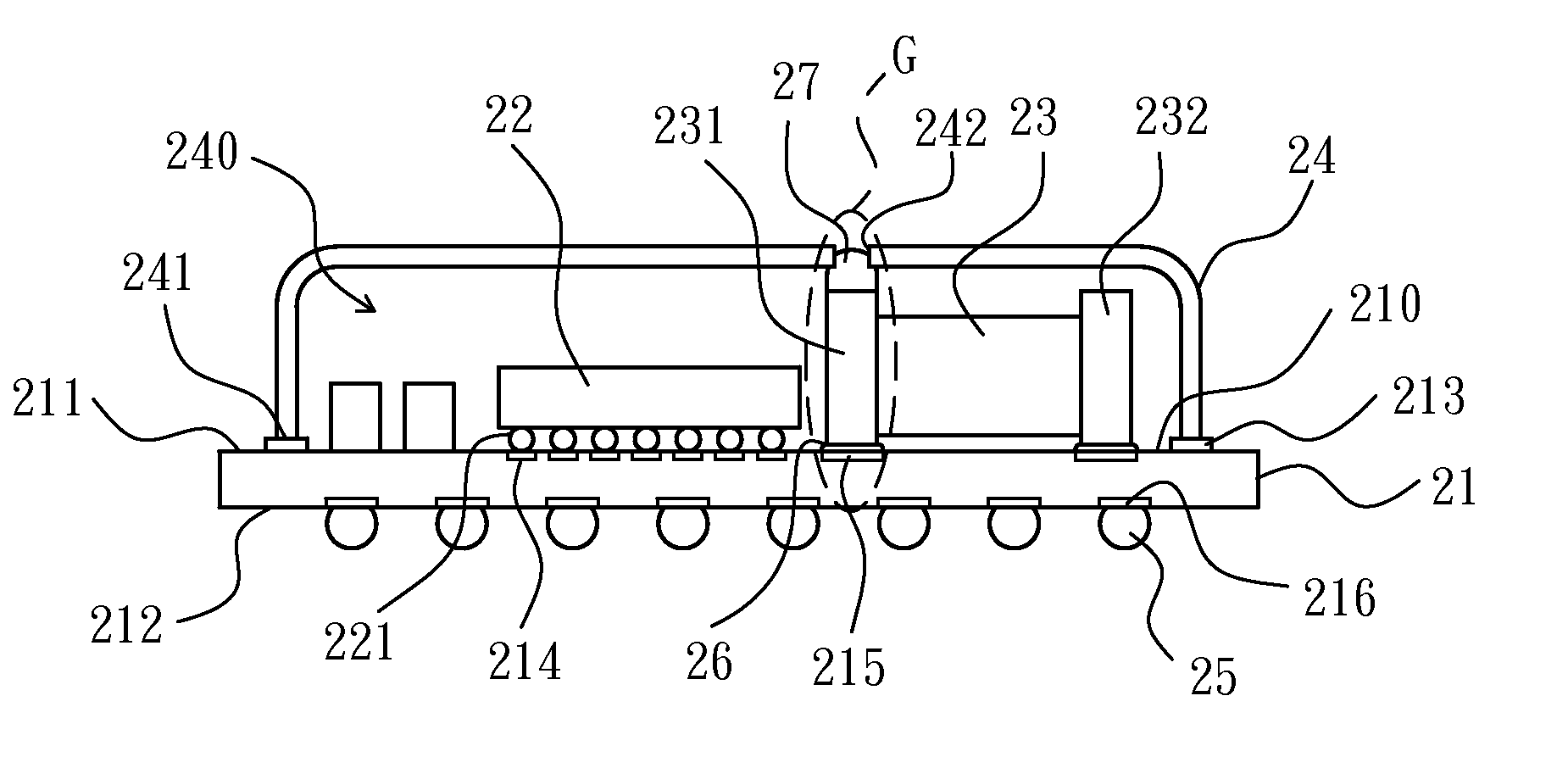
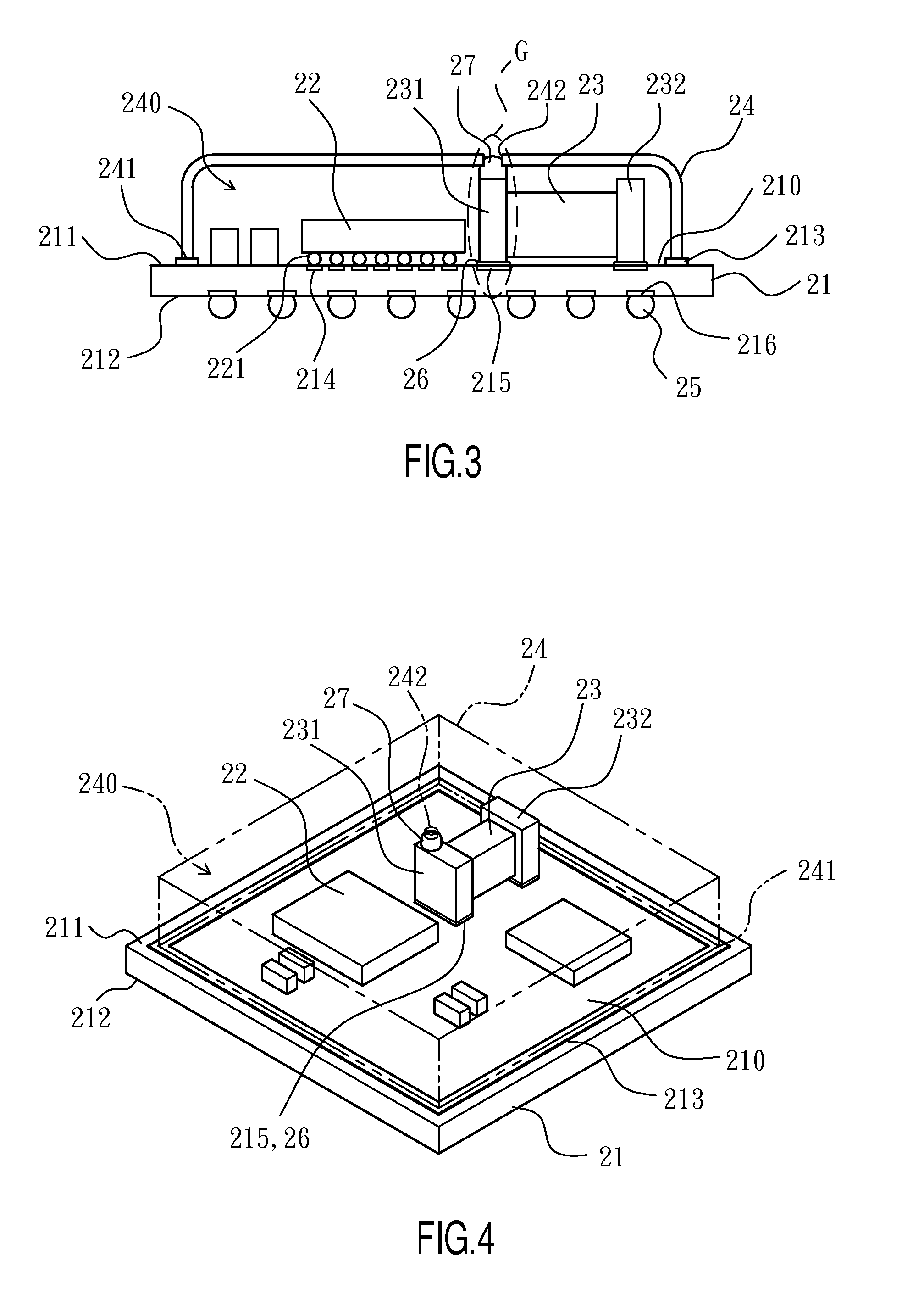
[0031]Referring now to FIGS. 3 and 4, a package structure for a wireless communication module according to a first embodiment of the present invention is illustrated. As shown, the package structure comprises a substrate 21, at least one chip 22, at least one electronic component 23 and a shielding lid 24. According to the amount of the chip 22, the package structure of the present invention can be constructed into a mono-chip-module structure or a multi-chip-module structure for the wireless communication module, which is suitably applied to various standard rules of wireless communication, such as WiMAX, Wi-Fi, Blue-Tooth and etc., but not limited thereto.

[0032]Referring to FIGS. 3 and 4, in the first embodiment of the present invention, the substrate 21 can be selected from a mono-layer or multi-layer structure of printed circuit board or ceramic circuit board. The substrate 21 has an upper surface 211 and a lower surface 212, wherein the upper surface 211 is defined with a suppo...


PUM


Abstract

A package structure for a wireless communication module is disclosed and includes: a substrate having an upper surface defining a supporting region, an annular ground pad surrounding the supporting region, and at least one auxiliary ground pad formed in the supporting region; at least one chip mounted on the supporting region and electrically connected to the substrate; and a shielding lid having a receiving space for receiving the chip, a ground end surface electrically connected to the annular ground pad of the substrate, and at least one auxiliary ground portion electrically connected to the auxiliary ground pad for forming at least one auxiliary ground pathway to adjust the characteristic of the enhanced peak generated by the cavity-resonance effect of the shielding lid. Thus, the enhanced peak can be shifted out of a regulated frequency range of the EMI shielding test, so that the yield thereof can be increased.

Description

FIELD OF THE INVENTION[0001]The present invention relates to a package structure for a wireless communication module, and more particularly to a package structure for reducing the effect of cavity resonance in a wireless communication module.BACKGROUND OF THE INVENTION[0002]Recently, the manufacturers of semiconductor assembly gradually develop various different package structures for satisfying needs of various high-density assembly, wherein various different design concepts of system-in-package (SIP) structures are frequently used to construct package structures for wireless communication modules, which will be applied to various electronic devices (such as mobile phones or global positioning system, GPS) which need wireless communication functions. Generally, the SIP structure can be classified into multi-chip-module (MCM) structure, package-on-package (POP) structure, package-in-package (PIP) structure and etc. The MCM structure includes a substrate, a plurality of chips mounted...

Claims


Application Information

Patent Timeline
IPC IPC(8): H01L23/552
CPCH01L23/552H01L24/16H01L25/16H01L2924/01079H01L2924/15311H01L2224/16225H01L2924/19041H01L2924/19042H01L2924/19043H01L2924/19105H01L2924/3025H01L2924/16152H01L2924/12041H01L2924/1615H01L2924/16251H01L2924/00
Inventor LIAO, KUO-HSIENLI, DIAN-RUNG
Owner ADVANCED SEMICON ENG INC
Why Eureka
Try Eureka