Solid-state imaging device, method of manufacturing the same, and electronic apparatus

a technology of solid-state imaging and manufacturing methods, applied in the direction of final product manufacturing, sustainable manufacturing/processing, television systems, etc., can solve the problems of difficult formation of light-shielding films deep in the substrate, inability to completely prevent the incidence of tilted light, and smear, so as to reduce the generation of mg flare, reduce the effect of optical color mixing and improvement of image quality

Active Publication Date: 2010-08-12
SONY CORP
View PDF14 Cites 423 Cited by
  • Summary
  • Abstract
  • Description
  • Claims
  • Application Information

AI Technical Summary

Benefits of technology

[0024]Under the reflection of above-described points, the invention is to provide a solid-state imaging device, a method of manufacturing the same, and an electronic apparatus, which improve image quality by reduction of optical color mixing and / or Mg flare.
[0025]The invention is to provide a back-illuminated solid-state imaging device and a method of manufacturing the same, which improves light-collecting property, and suppresses optical noise such as flare or smear. In addition, the invention provides an electronic apparatus including the solid-state imaging device.

Problems solved by technology

In such solid-state imaging device, there are problems that aliasing is generated in a semiconductor substrate by tilted incident light or incident light diffusely reflected in the upper portion of the light-receiving portion, and optical noise such as smear, flare is generated.
Since the CCD type solid-state imaging device in Japanese Unexamined Patent Application Publication No. 2004-140152 is constituted to form the light-shielding film in the groove portion formed using the LOCOS oxide film, it is difficult to form the light-shielding film deep in the substrate, and not possible to completely prevent incidence of tilted light, which is a cause of smear.
In addition, since the pixel area is reduced in proportion to the burying depth of the light-shielding film, it is practically difficult to bury deep the light-shielding film.
However, the distance between the substrate and the on-chip lens side is lengthened in proportion to the height of the light-shielding film, and thus deterioration of light-collecting property may occur.
When the light-collecting property is deteriorated, problems may occur such that the tilted light transmitted through a color filter of other pixels is incident to the light-receiving portion of different pixels from the pixels, and color mixing and sensitivity reduction are also generated.
(1) It is very difficult to completely suppress optical color mixing with adjacent pixel.
However, the light-collecting state changes in the effective pixel peripheral portion by level difference of the light-shielding film, and thus uniform optical property is not realized.
However, Mg flare 141, which is unique in the back-illuminated solid-state imaging device, is noticeable in comparison to the back green, for example, when photographing is taken for sunbeams streaming through leaves, and becomes problems.
However, optical color mixing to adjacent pixel may happen also in the front-illuminated solid-state imaging device.

Method used


Image

  • Solid-state imaging device, method of manufacturing the same, and electronic apparatus
  • Solid-state imaging device, method of manufacturing the same, and electronic apparatus
  • Solid-state imaging device, method of manufacturing the same, and electronic apparatus

Examples


first embodiment

2. First Embodiment

Configuration Example of Solid-State Imaging Device

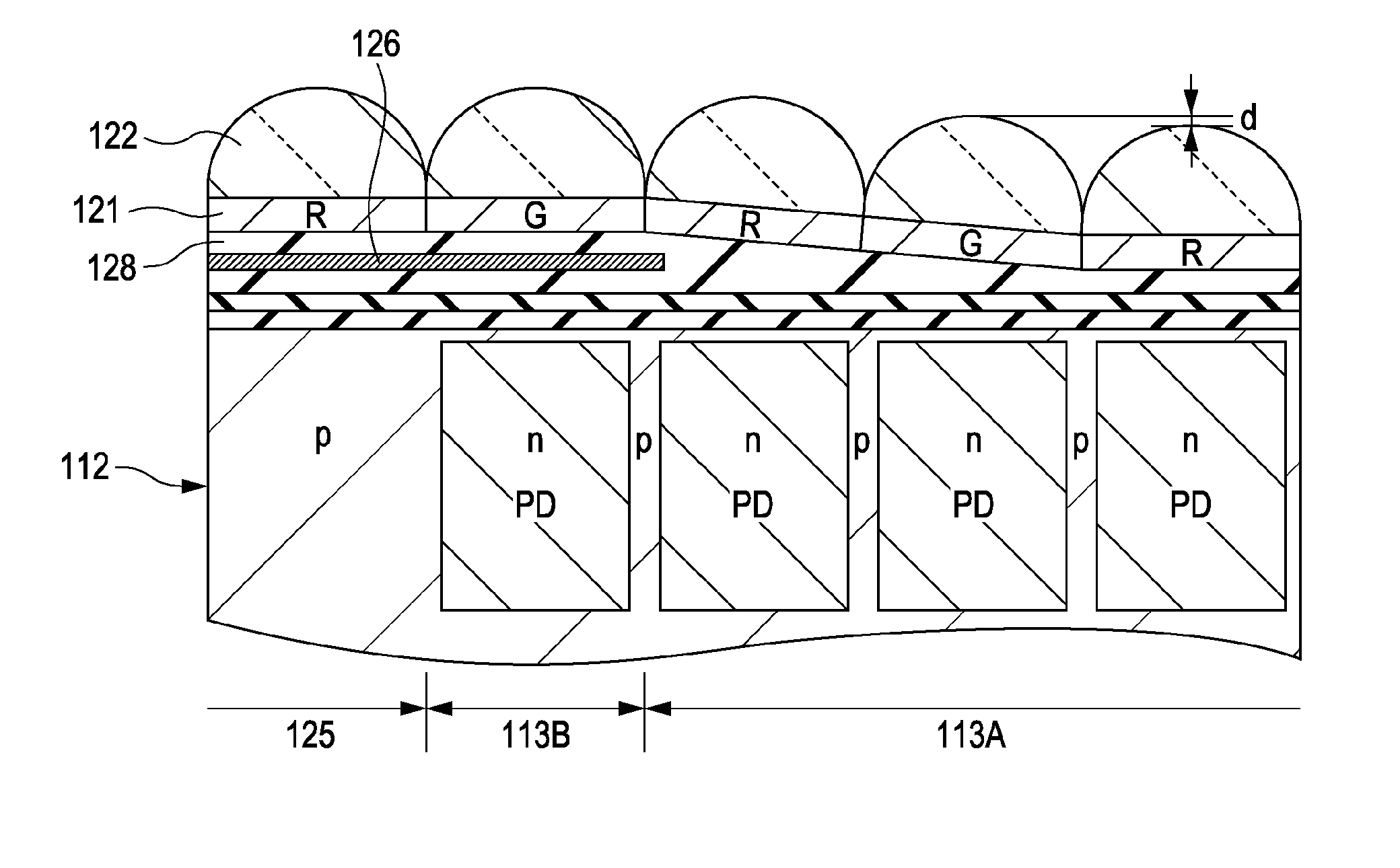
[0131]FIG. 8 shows the first embodiment of the solid-state imaging device according to the invention. The solid-state imaging device according to the embodiment is a back-illuminated CMOS solid-state imaging device. The solid-state imaging device 21 according to the first embodiment forms, for example, a pixel region (so-called image capturing region) 23 in which a plurality of pixels is arranged in a semiconductor substrate 22 made of silicon, and a peripheral circuit section (not shown) disposed in a periphery of the pixel region 23. A unit pixel 24 is constituted by a photodiode PD used as a photoelectric conversion section and a plurality of pixel transistors Tr. The photodiode PD is formed so as to extend over the whole region in a thickness direction of the semiconductor substrate 22, and is configured as a p-n junction type photodiode composed of a first conductivity type, which is an n-type semiconductor r...

second embodiment

3. Second Embodiment

Configuration Example of Solid-State Imaging Device

[0151]FIG. 14 shows the second embodiment of the solid-state imaging device according to the invention. The solid-state imaging device according to the embodiment is a back-illuminated CMOS solid-state imaging device. Similar to the first embodiment, the solid-state imaging device 51 according to the second embodiment forms, for example, a pixel region 23 in which a plurality of pixels is arranged in a semiconductor substrate 22 made of silicon, and a peripheral circuit section (not shown) disposed in a periphery of the pixel region 23. A logic circuit is formed in the peripheral circuit section. A unit pixel 24 is constituted by a photodiode PD used as a photoelectric conversion section and a plurality of pixel transistors Tr. The photodiode PD is formed so as to extend over the whole region in a thickness direction of the semiconductor substrate 22, and is configured as a p-n junction type photodiode composed o...

third embodiment

4. Third Embodiment

Configuration Example of Solid-State Imaging Device

[0176]FIG. 18 shows the third embodiment of the solid-state imaging device according to the invention. The solid-state imaging device according to the embodiment is a back-illuminated CMOS solid-state imaging device. The solid-state imaging device 56 according to the third embodiment is constituted so that each of the photodiodes PD is formed in the pixel region 23 of the semiconductor substrate 22, a logic circuit (not shown) is formed in the peripheral circuit section 57, and the antireflection film 36 and the insulating film 52 are formed on the backside 22B of the semiconductor substrate 22 in order.

[0177]In the embodiment, the lattice-shaped light-shielding film 39 in the pixel boundary is formed on the insulating film 52 corresponding to the pixel region 23, and the consecutive light-shielding film 39 is formed on the insulating film 52 corresponding to the peripheral circuit section 57 and an optical black ...


PUM


Abstract

A solid-state imaging device includes: a pixel region in which a plurality of pixels composed of a photoelectric conversion section and a pixel transistor is arranged; an on-chip color filter; an on-chip microlens; and a multilayer interconnection layer in which a plurality of layers of interconnections is formed through an interlayer insulating film. The solid-state imaging device further includes a light-shielding film formed through an insulating layer in a pixel boundary of a light receiving surface in which the photoelectric conversion section is arranged.

Description

BACKGROUND OF THE INVENTION[0001]1. Field of the Invention[0002]The invention relates to a solid-state imaging device, a method of manufacturing the same, and an electronic apparatus such as a camera including the solid-state imaging device.[0003]2. Description of the Related Art[0004]A digital video camera or digital still camera which is for use by consumers has called for high resolution power to transmit details of a photographic subject and a reduced-size device with a regard to portability. In addition, in order to realize these demands, development on a reduction in the pixel size while maintaining the image capturing property has been performed in regard to a solid-state imaging device (image sensor). However, in recent years, in addition to existing demands for high resolution and reduction in size, demand has been increasing for improvement in low luminance for photographic subjects or high-speed image capturing and the like. In order to realize these, expectation has incr...

Claims


Application Information

Patent Timeline
Patent Type & Authority Applications(United States)
IPC IPC(8): H04N5/228H04N5/335H04N5/225H01L31/18
CPCH01L21/7806H01L27/1464H01L27/14627H01L27/1463H01L27/14632H01L27/14645H01L27/14685H01L27/14687H01L31/02162H01L31/1804H01L27/14612H01L27/14636H01L27/14621H04N5/359H01L27/14629H01L27/14623Y02P70/50H04N25/62H01L31/0216H01L31/18
Inventor MARUYAMA, YASUSHIWATANABE, KAZUFUMI
Owner SONY CORP
Why Eureka
Try Eureka