Chiplet display device with serial control

a display device and serial control technology, applied in the field of display devices, can solve the problems of limited number of rows (or columns) of passive-matrix drive devices, limited lifetime and power consumption of passive-matrix devices, and limited number of rows (or columns) of passive-matrix devices, so as to improve the aperture ratio, simplify the control method of a display, and improve the effect of life and power consumption

Active Publication Date: 2010-08-19
GLOBAL OLED TECH
View PDF13 Cites 39 Cited by
  • Summary
  • Abstract
  • Description
  • Claims
  • Application Information

AI Technical Summary

Benefits of technology

[0018]The present invention has the advantage of a simpler control method for a display. A further advantage is that the aperture ratio, and therefore the lifetime and power consumption, are improved compared to the prior art.

Problems solved by technology

However, a passive-matrix drive device is limited in the number of rows (or columns) that can be included in the device since the sequential nature of the row (or column) driving creates flicker.
If too many rows are included, the flicker can become perceptible.
Typically, passive-matrix devices are limited to about 100 lines, far fewer than is found in contemporary large-panel displays, for example such as high-definition televisions that have over 1,000 lines and are therefore unsuitable for passive-matrix control.
Moreover, the currents necessary to drive an entire row (or column) in a passive-matrix display can be problematic and limits the physical size of a passive-matrix display.
Furthermore, the external row and column driver chips for both passive- and active-matrix displays are expensive.
This technique is used because other schemes such as direct addressing (for example as used in memory devices) require the use of address decoding circuitry that is very difficult to form on a conventional thin-film active-matrix backplane and impossible to form on a passive-matrix backplane.
Moreover, the logic required to support such data shifting would require so much space in a conventional thin-film transistor active-matrix backplane that the resolution of the device would be severely limited and is impossible in a passive-matrix backplane.
Thin-film transistors (TFTs) made from amorphous or polycrystalline silicon are relatively large and have lower performance compared to conventional transistors made in crystalline silicon wafers.
Moreover, such thin-film devices typically exhibit local or large-area non-uniformity across the glass substrate that results in non-uniformity in the electrical performance and visual appearance of displays employing such materials.
The wiring for the signals takes up a considerable area on a substrate, thereby reducing the aperture ratio or increasing the number of metal layers on the substrate and the cost, and is limited in the frequency at which it can operate and the current that can be employed.
A matrix-addressing pixel control technique is taught and therefore suffers from the same limitations as noted above.

Method used


Image

  • Chiplet display device with serial control
  • Chiplet display device with serial control
  • Chiplet display device with serial control

Examples


Embodiment Construction

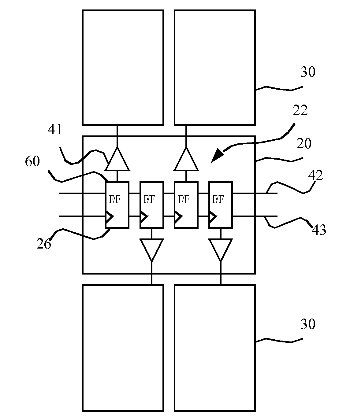
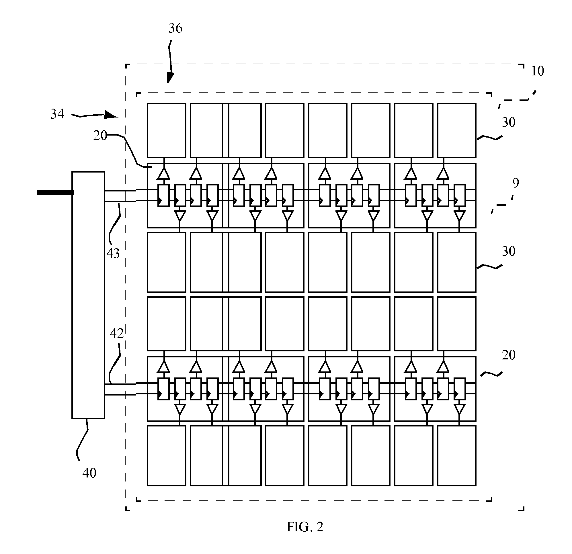
[0029]Referring to FIGS. 1, 2, and 3 in one embodiment of the present invention, a display device includes a substrate 10 and an array of pixels 30 forming a light-emitting area 9 over the substrate 10, the array of pixels 30 arranged in rows 34 and columns 36 formed on the substrate 10. Referring to FIG. 3, each pixel 30 includes a first electrode 12, one or more layers of light-emitting or light-controlling material 14 located over the first electrode 12, and a second electrode 16 located over the one or more layers of light-emitting material 14. The layers 12, 14 and 16 include a pixel 30, for example an organic light-emitting diode 15, in the areas where all three layers 12, 14, 16 overlap and current can flow through the one or more layers of light-emitting or light-controlling material 14 from the electrodes 12, 16.

[0030]A first serial buss 42 has a plurality of electrical conductors, each electrical conductor connecting one chiplet 20 in a first set of chiplets to only one ot...


PUM


Abstract

A display device, including a substrate; an array of pixels arranged in rows and columns forming a light-emitting area over the substrate, each pixel including a first electrode, one or more layers of light-emitting material located over the first electrode, and a second electrode located over the one or more layers of light-emitting material; a first serial buss having a plurality of electrical conductors, each electrical conductor connecting one chiplet in a first set of chiplets to only one other chiplet in the first set in a serial connection, the chiplets being distributed over the substrate in the light-emitting area, each chiplet including one or more store-and-forward circuits for storing and transferring data connected to its corresponding electrical conductor; and a driver circuit in each chiplet for driving at least one pixel in response to data stored in the store-and-forward circuit.

Description

FIELD OF THE INVENTION[0001]The present invention relates to display devices having a substrate with distributed, independent chiplets employing serial control for a pixel array.BACKGROUND OF THE INVENTION[0002]Flat-panel display devices are widely used in conjunction with computing devices, in portable devices, and for entertainment devices such as televisions. Such displays typically employ a plurality of pixels distributed over a substrate to display images. Each pixel incorporates several, differently colored light-emitting elements commonly referred to as sub-pixels, typically emitting red, green, and blue light, to represent each image element. As used herein, pixels and sub-pixels are not distinguished and refer to a single light-emitting element. A variety of flat-panel display technologies are known, for example plasma displays, liquid crystal displays, and light-emitting diode (LED) displays.[0003]Light emitting diodes (LEDs) incorporating thin films of light-emitting mate...

Claims


Application Information

Patent Timeline
Patent Type & Authority Applications(United States)
IPC IPC(8): G09G3/30
CPCG09G3/2085G09G2300/0426G09G2300/026G09G3/3208G09G3/32G09G3/30
Inventor COK, RONALD S.
Owner GLOBAL OLED TECH
Why Eureka
Try Eureka