Semiconductor device with process monitor circuit and test method thereof

a technology of process monitor and semiconductor device, which is applied in the direction of semiconductor/solid-state device details, pulse technique, instruments, etc., can solve the problems of affecting the accuracy of the test method, and affecting the design freedom, etc., and achieves the effect of high accuracy and short measurement tim

Inactive Publication Date: 2005-02-08
RENESAS ELECTRONICS CORP
View PDF10 Cites 34 Cited by
  • Summary
  • Abstract
  • Description
  • Claims
  • Application Information

AI Technical Summary

Benefits of technology

The present invention has been made to solve the above-described problems, and has an object of providing a semiconductor device capable of appropriately debugging any fluctuation even in the case that any element characteristic fluctuates exceeding a value estimated at the designing stage, thus preventing operation margin of any circuit element from being reduced due to fluctuation in process, improving freedom in design, and reducing production of defective product.
Another object of the invention is to apply a simple control method to a process monitor circuit itself that monitors the fluctuation in element characteristic due to the process variation thereby making it possible to put the process monitor circuit into practical use.
As a result of employing such arrangement, in the manufacturing process of the semiconductor device, even when any characteristic of the circuit element fluctuates exceeding a value estimated at the designing stage, operation timing of the circuit element affected by the fluctuation in process can be appropriately controlled. Accordingly, it becomes possible to prevent operation margin of the circuit element from being reduced thereby improving a degree of freedom in designing.
As a result, without any special and dedicated external device, fluctuation in the manufacturing process of the semiconductor device can be monitored using a simple general-purpose semiconductor test apparatus. In particular, simple control on a command base by means of the control section becomes possible, and the measurement will be simple. Further, development time and development cost of any program, etc. for the purpose of measurement is reduced. In addition, a large number of control terminals are not required, thereby any expensive overhead charge on the product applied with the semiconductor device is not required.
As a result, in the test method of the invention, without any special and dedicated external device, a delay time of psec order can be measured in a short time as well as at a high accuracy using a simple and general-purpose semiconductor test apparatus.

Problems solved by technology

However, in the case of any large variation in process conditions, there is a possibility that the characteristic of the circuit element fluctuates exceeding a value estimated preliminarily at the stage of designing.
In such a case, with no way for any debug, there has been no alternative but to scrap it as a defective item.
Moreover, since it is necessary to consider the fluctuation in element characteristic due to the process variation whenever designing the semiconductor device, restriction such as timing control to secure an operation margin of the circuit element becomes large resulting in a restriction on the freedom in design.
However, the mentioned conventional technique only makes it possible to monitor what level of fluctuation in element characteristic of the semiconductor device is generated due to the variation in process conditions, and never makes it possible to automatically debug the semiconductor device itself in which the fluctuation in process actually occurs.
Therefore, when any element characteristic fluctuates exceeding a value estimated at the designing stage, there has been no choice but scrapping the semiconductor device as a defective item.
Moreover, since it is necessary to consider the fluctuation in element characteristic due to the process variation whenever designing the semiconductor device, a large restriction on the operation timing becomes large.
Consequently a problem exists in that freedom in the design is still limited.
(See the Japanese Patent Publication (unexamined) No. 12639 / 2000, the Japanese Patent Publication (unexamined) No. 127186 / 1997, etc.) That is, in order to apply such known circuit to the semiconductor device, it is required to increase number of terminals, and because control of the process monitor circuit is not always simple, a further problem exits in that manufacturing cost of the semiconductor device is raised.

Method used


Image

  • Semiconductor device with process monitor circuit and test method thereof
  • Semiconductor device with process monitor circuit and test method thereof
  • Semiconductor device with process monitor circuit and test method thereof

Examples


embodiment 1

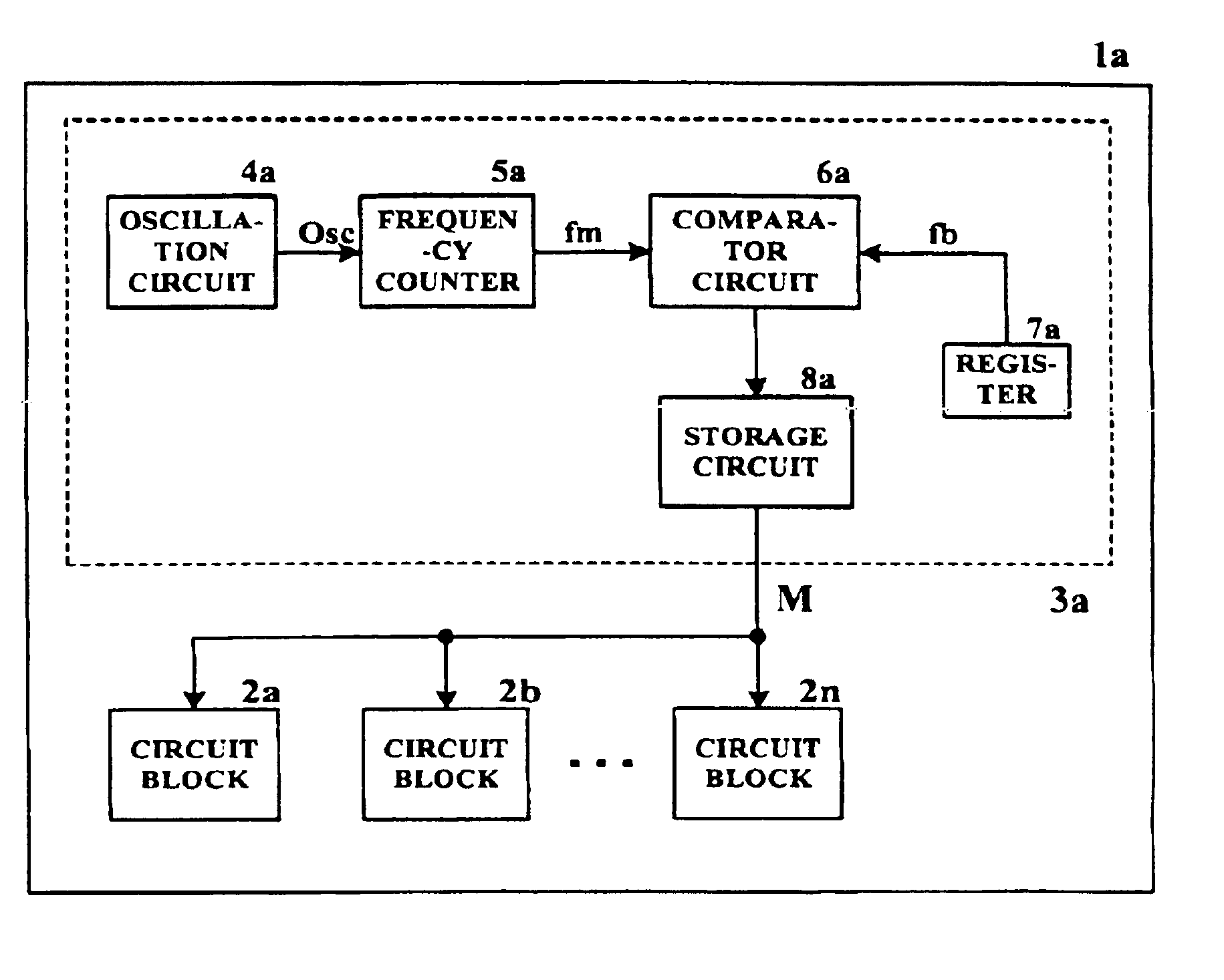
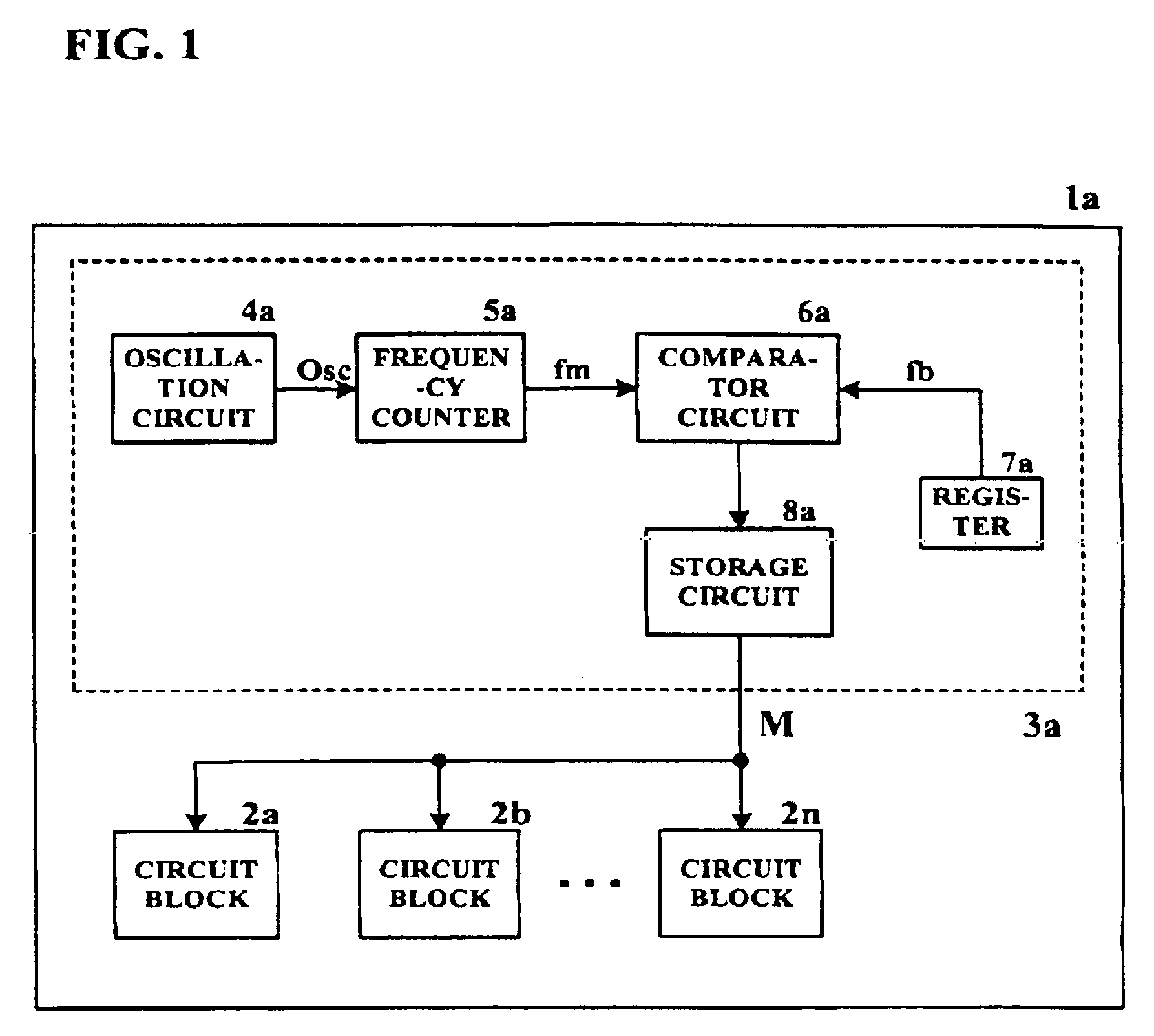
FIG. 1 is a block diagram showing an arrangement of a semiconductor device according to Embodiment 1 of the present invention.

In this semiconductor device according to Embodiment 1, on the same semiconductor chip 1a, a plurality of circuit blocks 2a to 2n that individually perform required functions are provided. In addition to these circuit blocks 2a to 2n, a process monitor circuit 3a that monitors fluctuation in process and outputs a monitor signal M indicating a result thereof (1 bit of data in this example), is also mounted thereon.

Taking a case of DRAM as an example, equivalent to the above-described respective circuit blocks 2a to 2n are timing signal generation circuit for writing or reading out, address signal generation circuit, refresh signal generation circuit and the like.

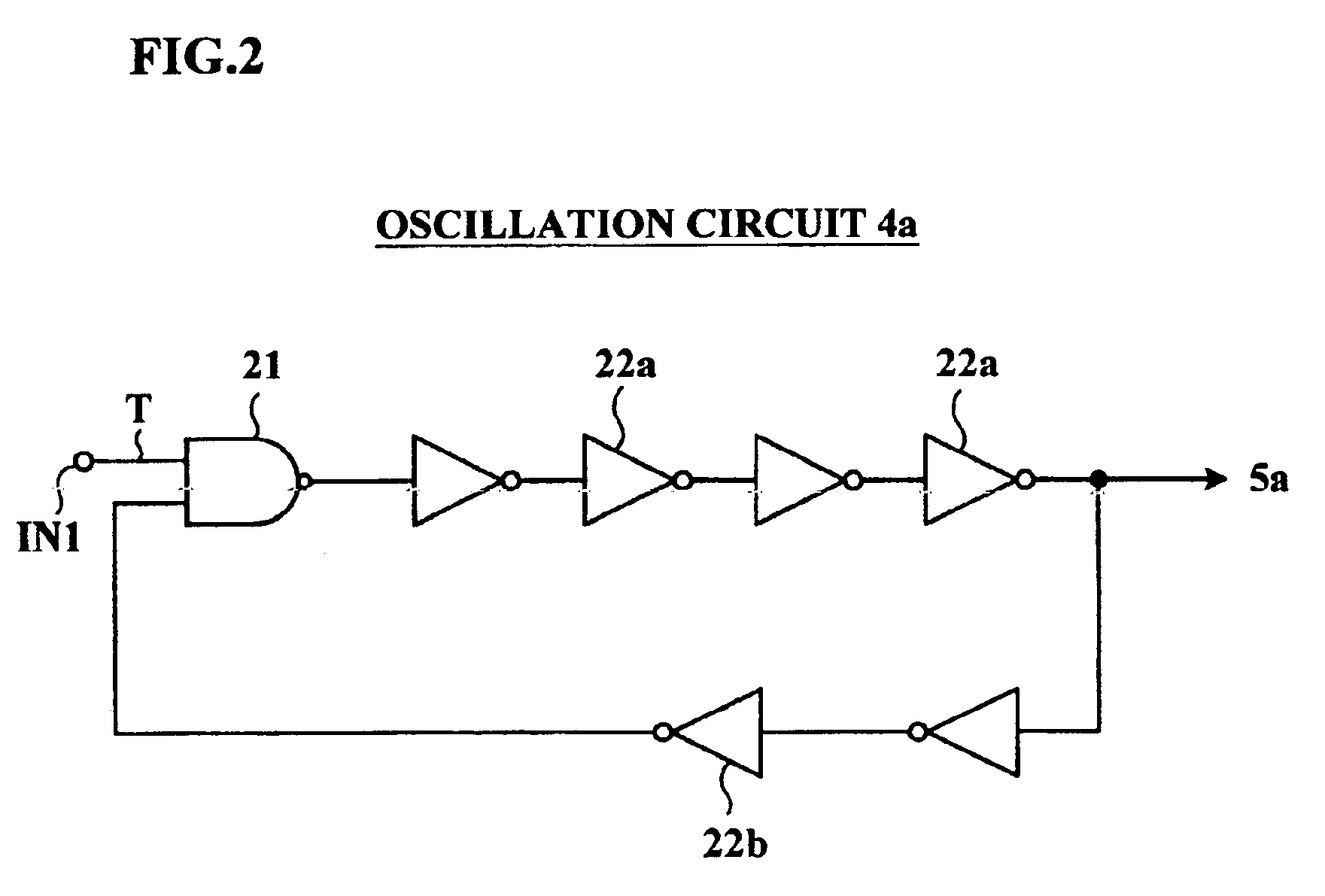
Further, the process monitor circuit 3a is provided with an oscillation circuit 4a that oscillates at a predetermined frequency, a frequency counter 5a that measures an oscillation frequency Osc of the...

embodiment 2

FIG. 5 is a block diagram showing an arrangement of the semiconductor device provided with a process monitor circuit according to Embodiment 2 of the invention.

In the semiconductor device according to this second embodiment, in order to improve accuracy in monitoring the process fluctuation in element characteristic, the arrangement of the process monitor circuit (FIG. 1) according to the foregoing Embodiment 1 is modified.

That is, in this second embodiment, on the same semiconductor chip 1b, a plurality of circuit blocks 2a to 2n that individually perform required functions are provided. In addition to these circuit blocks 2a to 2n, a process monitor circuit 3b that monitors fluctuation in process is also mounted thereon. Further, this process monitor circuit 3b is provided with an oscillation circuit 4b that oscillates at mutually different frequencies respectively in response to a selection signal Se supplied from outside.

This oscillation circuit 4b, as shown in FIG. 6, is provid...

embodiment 3

FIG. 11 is a block diagram showing an arrangement of the semiconductor device provided with a process monitor circuit according to Embodiment 3 of this invention.

In the semiconductor device according to this embodiment, at least one process monitor circuit 300 that monitors the fluctuation in process and outputs a result thereof to outside is mounted on the same semiconductor chip or in the vicinity of the semiconductor chip on the semiconductor wafer.

In this embodiment, the process monitor circuit 300 is provided with an oscillation circuit 400 that oscillates at a predetermined frequency, a frequency counter 500 that measures oscillation frequency of the oscillation circuit 400, and a control section 600 that is connected to the oscillation circuit 400 and to the frequency counter 500 and controls operation sequence of the whole process monitor circuit 300.

As the above-described oscillation circuit 400, for example, as shown in FIG. 12, a ring oscillator is used. The ring oscillat...


PUM


Abstract

The invention provides a semiconductor device capable of appropriately debugging any fluctuation in element characteristic even when the element characteristic fluctuates exceeding a value estimated at the designing stage. This semiconductor device includes a process monitor circuit that monitors any fluctuation in process and outputs a monitor signal M representing a result of monitoring, in addition to circuit blocks that perform respectively required functions. And a timing control circuit that controls timing of an input signal inputted to a predetermined circuit element forming the circuit blocks based on the monitor signal M from the process monitor circuit is provided in the circuit blocks.

Description

BACKGROUND OF THE INVENTION1. Technical FieldThe present invention relates to a semiconductor device provided with a process monitor circuit in order to monitor fluctuation in circuit element characteristic due to any process change or variation and debug a result thereof, and a test method thereof.2. Background ArtGenerally, in manufacturing process of a semiconductor device, any fluctuation in characteristic is generated in any circuit element such as transistor that is an essential element of the semiconductor device or a logic gate formed in combination of the transistors due to variation in process conditions.To overcome this, design is usually carried out taking such a fluctuation in characteristic of the circuit element due to variation in process into account (the fluctuation is hereinafter referred to as “fluctuation in process” or “process fluctuation”). However, in the case of any large variation in process conditions, there is a possibility that the characteristic of the...

Claims


Application Information

Patent Timeline
Patent Type & Authority Patents(United States)
IPC IPC(8): H01L21/66G01R31/28G11C11/401G11C29/12H01L21/822H01L27/04H03K5/00
CPCH01L22/20H01L2924/0002H01L2924/00
Inventor SHIBAYAMA, MARIFUJIWARA, YOSHINORINAGURA, YOSHIHIRO
Owner RENESAS ELECTRONICS CORP
Why Eureka
Try Eureka