Photomultiplier tube

a technology of photomultiplier and tube, which is applied in the direction of electron multiplier details, multiplier electrode arrangement, electric discharge tube, etc., can solve the problems of reducing withstand voltage and easy multiplication of electrons, and achieve the effect of preventing a decrease in withstand voltage, preventing electrons from being incident onto and preventing electrons from being made incident on the surface of the substrate more effectively

Active Publication Date: 2010-08-26
HAMAMATSU PHOTONICS KK
View PDF7 Cites 17 Cited by
  • Summary
  • Abstract
  • Description
  • Claims
  • Application Information

AI Technical Summary

Benefits of technology

[0009]According to the above-described photomultiplier tube, incident light is made incident onto the photocathode and converted to photoelectrons, and the photoelectrons are made incident onto the electron multiplying part constituted with a plurality of stages on the substrate and multiplied accordingly, and the thus multiplied electrons are taken out as an electric signal from the anode part. In this instance, an insulative groove is formed on the surface of the substrate between adjacent stages of the electron multiplying part, thus making it possible to prevent electrons passing between adjacent stages of the electron multiplying part from being made incident onto the surface of the substrate. It is, thereby, possible to prevent a decrease in withstand voltage due to electric charge on the surface of the substrate.
[0010]It is preferable that the groove is formed over a range held between the edge part of a K−1th stage electron multiplying part on the second end side and the edge part of a Kth stage (K denotes an integer of 2 or more but N or less) electron multiplying part on the first end side. In this instance, the orbit of electrons between adjacent stages of the electron multiplying part can be reliably separated from the surface of the substrate, thus making it possible to effectively prevent electrons from being made incident onto the surface of the substrate.
[0011]It is also preferable that the groove is formed so as to spread to the second end side more than the edge part of the Kth stage electron multiplying part on the first end side. According to the above-described constitution, electrons passing between adjacent stages of the electron multiplying part are made incident onto the second end side of the groove to a smaller extent, thus making it possible to prevent electrons from being made incident onto the surface of the substrate more effectively.
[0012]Further, it is preferable that the groove is formed so as to spread to the first end side more than the edge part of the K−1th stage electron multiplying part on the second end side. In this instance, electrons passing through adjacent stages of the electron multiplying part are made incident onto the first end side of the groove to a smaller extent, thus making it possible to prevent electrons from being made incident onto the surface of the substrate more effectively.
[0013]Still further, it is preferable that a groove which communicatively connects between adjacent grooves at the end parts of the raised parts is also formed on the flat surface of the substrate. Thereby, the electron multiplying part on the raised parts is separated from the substrate to further improve a withstand voltage.

Problems solved by technology

However, in the above-described conventional photomultiplier tubes, there is a tendency that multiplied electrons are easily made incident on the surface of an insulating substrate installed between each adjacent stage of the dynodes.
Therefore, there has been a case where the insulating substrate is electrically charged to result in a decreased withstand voltage.

Method used


Image

  • Photomultiplier tube
  • Photomultiplier tube
  • Photomultiplier tube

Examples


Embodiment Construction

[0023]Hereinafter, a detailed description will be given for preferred embodiments of the photomultiplier tube related to the present invention by referring to drawings. In addition, in describing the drawings, the same or corresponding parts will be given the same reference numerals to omit overlapping description.

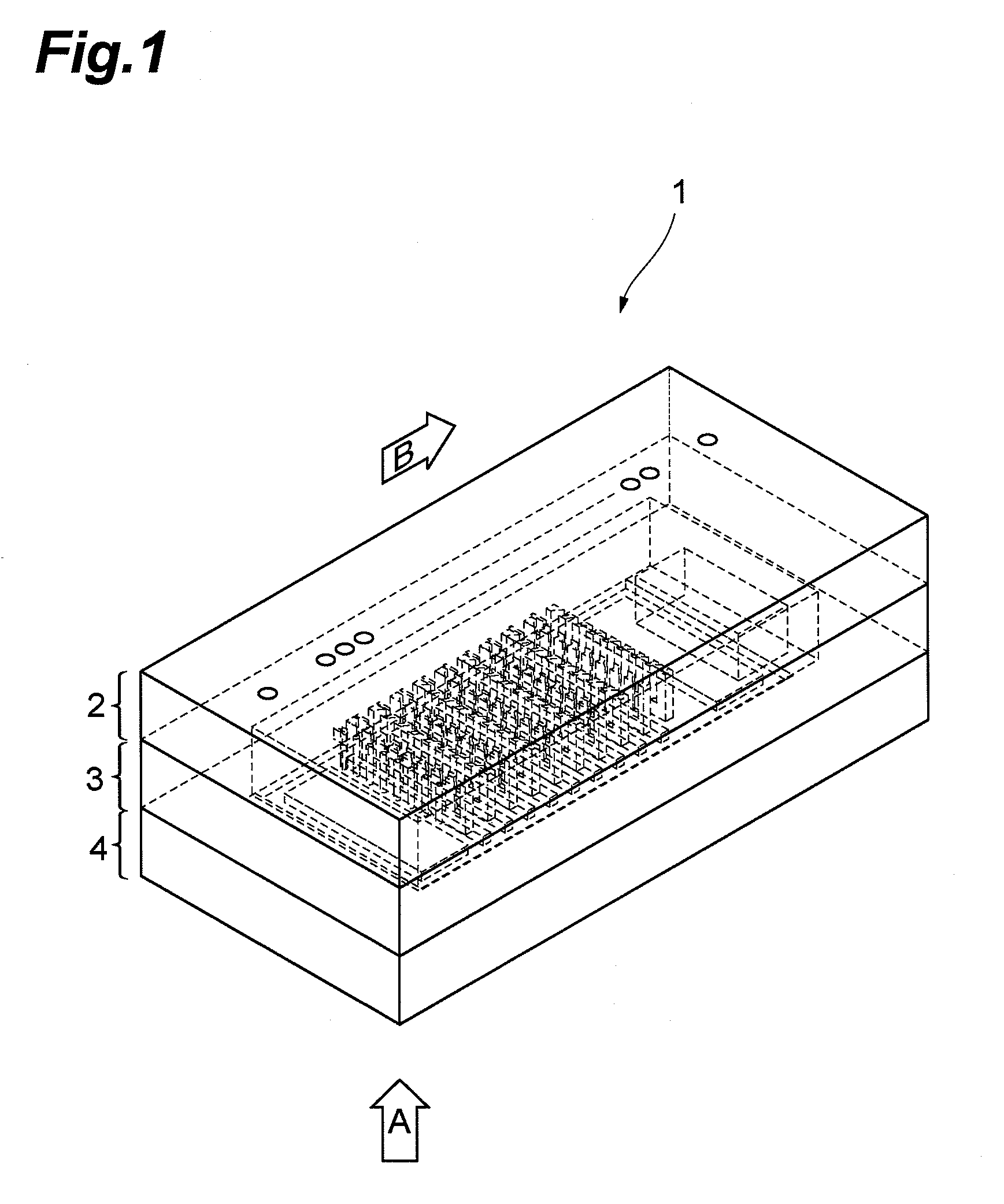
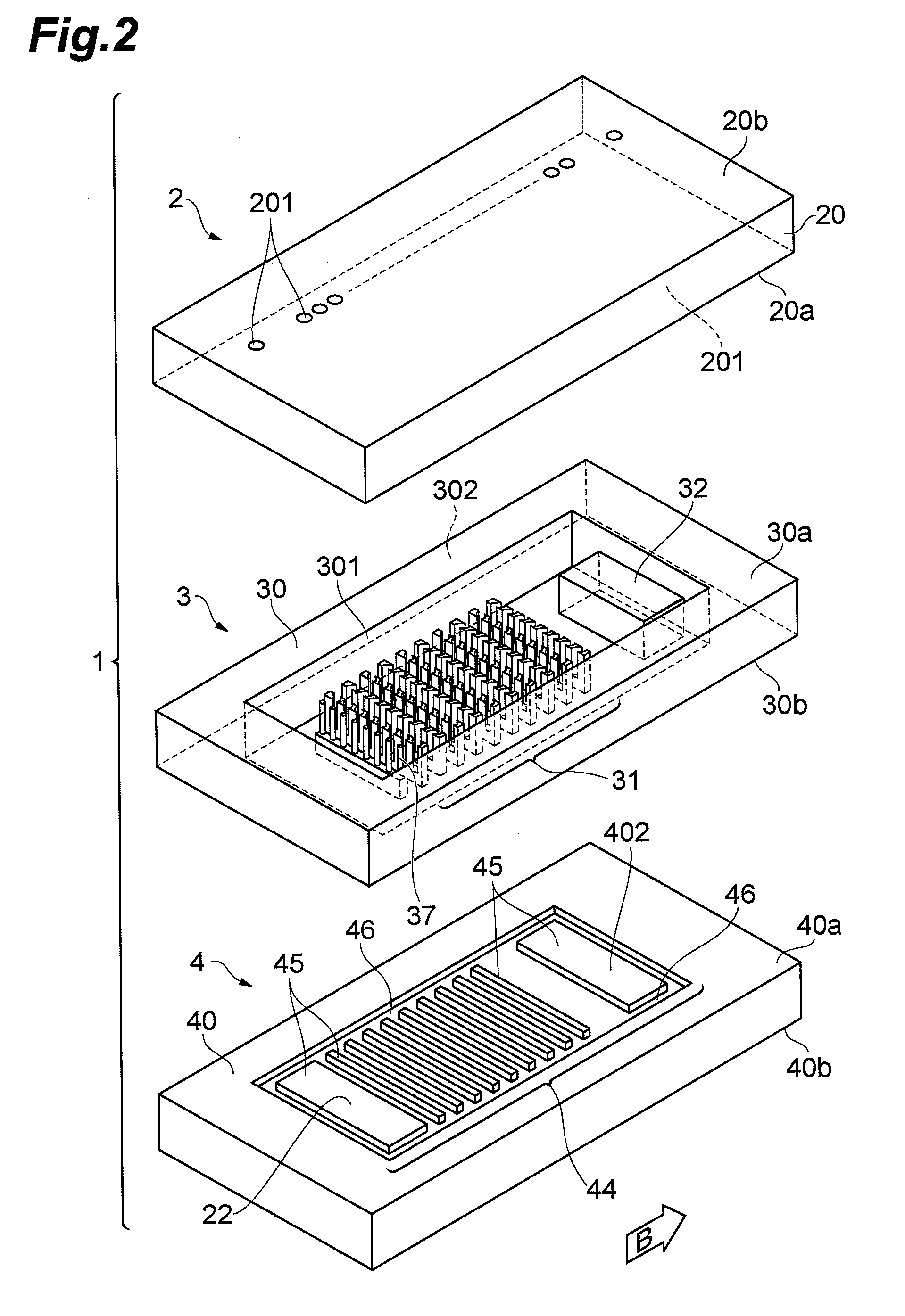
[0024]FIG. 1 is a perspective view of a photomultiplier tube 1 related to one preferred embodiment of the present invention. FIG. 2 is an exploded perspective view of the photomultiplier tube 1 in FIG. 1.

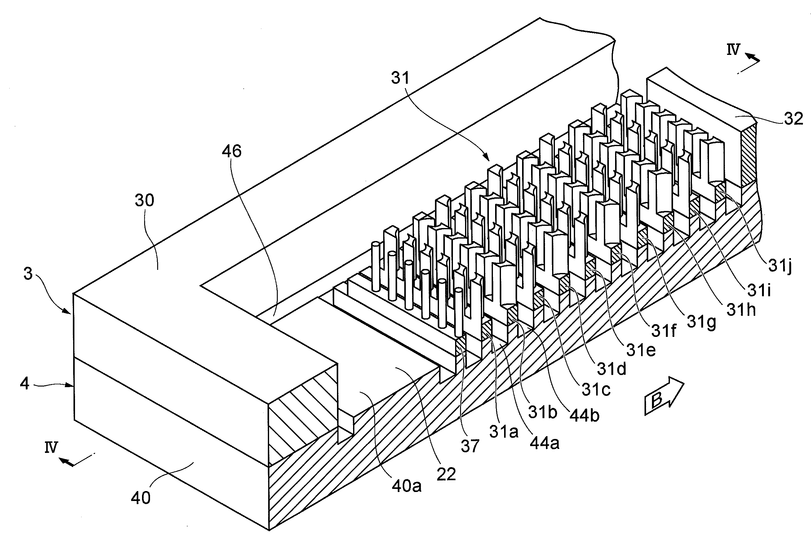
[0025]The photomultiplier tube 1 shown in FIG. 1 is a photomultiplier tube having a transmission-type photocathode and provided with a casing constituted with an upper frame 2 (glass substrate), a side-wall frame 3 (silicon substrate) and a lower frame 4 (glass substrate). The photomultiplier tube 1 is an electron tube such that a light incident direction onto the photocathode intersects with a direction at which electrons are multiplied at the electron multiplying part. S...


PUM


Abstract

Electrons are prevented from being made incident onto an insulation part between dynodes to improve a withstand voltage. The photomultiplier tube 1 is provided with a casing having a glass substrate 40 on which a main surface 40a made with an insulating material is formed, dynodes 31 constituted with a 1st stage to an Nth stage (N denotes an integer of 2 or more) which are arrayed so as to be spaced away sequentially from a first end side to a second end side on the main surface 40a, a photocathode 22 which is installed on the first end side so as to be spaced away from the 1st stage dynode 31a to emit photoelectrons, and an anode part 32 which is installed on the second end side so as to be spaced away from the Nth stage dynode 31j, taking out multiplied electrons as a signal, in which a groove 44, the surface of which is made with an insulating material, is formed between two adjacent dynodes 31 on the main surface 40a of the glass substrate 40, and the 1st stage to the Nth stage dynodes 31 are fixed on raised parts 45 adjacent to the grooves 44 on the glass substrate 40.

Description

BACKGROUND OF THE INVENTION[0001]1. Field of the Invention[0002]The present invention relates to a photomultiplier tube for detecting incident light from outside.[0003]2. Related Background Art[0004]Conventionally, compact photomultiplier tubes by utilization of fine processing technology have been developed. For example, a flat surface-type photomultiplier tube which is arranged with a photocathode, dynodes and an anode on a translucent insulating substrate is known (refer to Patent Document 1 given below). The above-described structure makes it possible to detect weak light at a high degree of reliability and also downsize a device.[0005]Patent Document 1: U.S. Pat. No. 5,264,693SUMMARY OF THE INVENTION[0006]However, in the above-described conventional photomultiplier tubes, there is a tendency that multiplied electrons are easily made incident on the surface of an insulating substrate installed between each adjacent stage of the dynodes. Therefore, there has been a case where the...

Claims


Application Information

Patent Timeline
Patent Type & Authority Applications(United States)
IPC IPC(8): H01J43/18
CPCH01J43/243
Inventor SUGIYAMA, HIROYUKISHIMOI, HIDEKIKODAMA, TSUYOSHIKISHITA, HITOSHIKOHNO, YASUYUKIINOUE, KEISUKE
Owner HAMAMATSU PHOTONICS KK
Why Eureka
Try Eureka