Surface-emitting laser array, optical scanning device, and image forming device

a laser array and surface-emitting technology, applied in semiconductor lasers, instruments, electrographic processes, etc., can solve the problems of laser output performance decline, device using four or eight beams in view of the cost, and large power dissipation

Active Publication Date: 2010-08-26
RICOH KK
View PDF32 Cites 40 Cited by
  • Summary
  • Abstract
  • Description
  • Claims
  • Application Information

AI Technical Summary

Benefits of technology

[0012]In one aspect of the invention, the present disclosure provides a surface-emitting laser array which is able to reduce the influence of heat generated in other light emitting parts without enlarging the size.
[0014]In one aspect of the invention, the present disclosure provides an image forming device which includes the surface-emitting laser array and is able to form a high-density image at high speed.
[0016]In the present disclosure, a spacing between two of the plurality of light emitting parts means a center-to-center distance between the two light emitting parts in one of the two orthogonal directions. The surface-emitting laser array of this invention makes it possible to selectively increase the spacing between two of the light emitting parts located in the area which is likely to receive the influences of heat from other light emitting parts. It is possible for the surface-emitting laser array of the invention to reduce the influence of heat generated in other light emitting parts, and it is not necessary to enlarge the size, in order to avoid the fall of the laser output performance due to the influence of heat.
[0017]In an embodiment of the invention which solves or reduces one or more of the above-mentioned problems, the present disclosure provides an optical scanning device comprising: a light source unit including the above-mentioned surface-emitting laser array, the light source unit having a main scanning direction and a sub-scanning direction parallel to the two orthogonal directions respectively; a deflection unit deflecting a plurality of laser beams emitted by the light source unit; and a scanning optical system focusing the laser beams output from the deflection unit on a scanned surface of a photoconductor. The optical scanning device of this invention includes the above-mentioned surface-emitting laser array, and it is possible to scan the surface of the photoconductor at high speed with high density.
[0018]In an embodiment of the invention which solves or reduces one or more of the above-mentioned problems, the present disclosure provides an image forming device comprising the above-mentioned optical scanning device and a photoconductor, wherein the optical scanning device scans a surface of the photoconductor by laser beams output from the optical scanning device, so that an image is formed on the photoconductor surface in accordance with image information of the laser beams. The image forming device of this invention includes the optical scanning device mentioned above, and it is possible to form a high-density image at high speed.
[0019]In an embodiment of the invention which solves or reduces one or more of the above-mentioned problems, the present disclosure provides an image forming device comprising the above-mentioned surface-emitting laser array, wherein the surface-emitting laser array is provided as a part of an optical writing unit, the optical writing unit outputting laser beams to a photoconductor when writing image information to the photoconductor. The image forming device of this invention includes the above-mentioned surface-emitting laser array, and it is possible to form a high-density image at high speed.

Problems solved by technology

In these cases, if the number of laser beams increases, the power dissipation becomes large, and it is necessary to arrange a cooling system for cooling the lasers.
Practically, the limitation may be the device using four beams or eight beams in view of the cost.
The surface-emitting laser array according to the related art has a problem that, if the spacing between two of the light emitting parts is shortened, the laser output performance may decline or the reliability may fall due to the influence of heat generated in other light emitting parts.

Method used


Image

  • Surface-emitting laser array, optical scanning device, and image forming device
  • Surface-emitting laser array, optical scanning device, and image forming device
  • Surface-emitting laser array, optical scanning device, and image forming device

Examples


Embodiment Construction

[0041]A description will be given of embodiments of the invention with reference to the accompanying drawings.

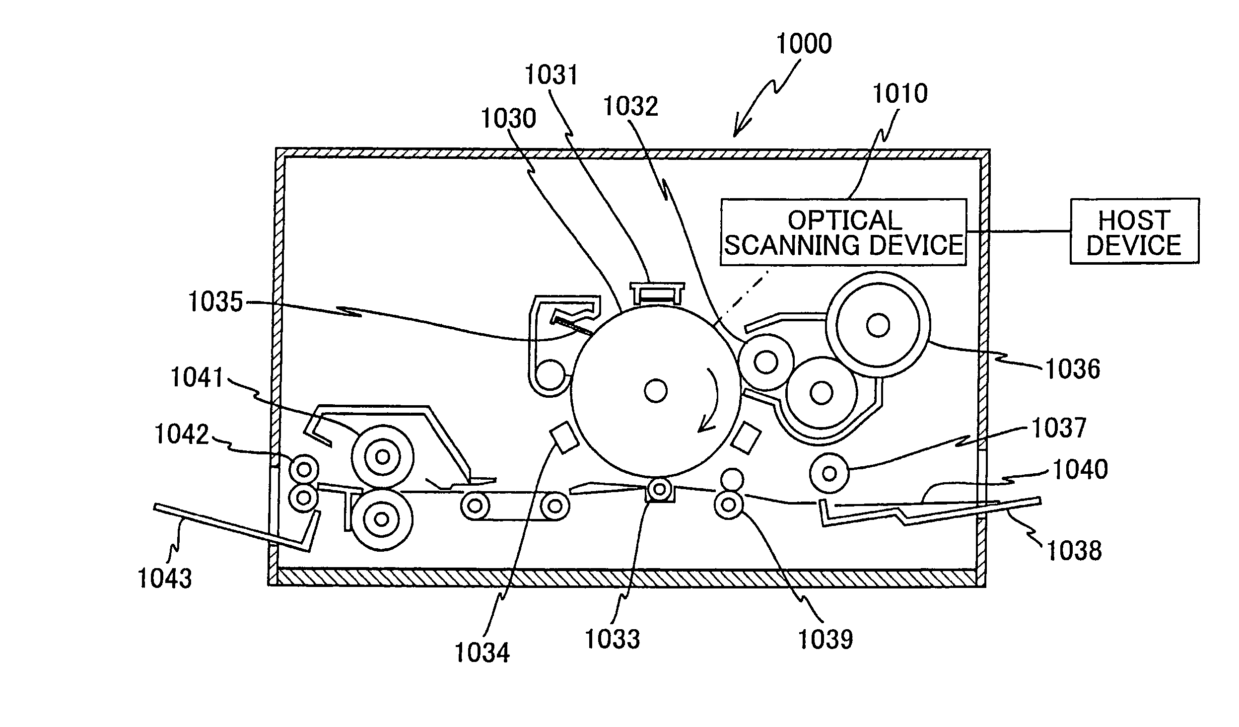
[0042]FIG. 1 shows the composition of a laser printer 1000 which is an image forming device in an embodiment of the invention. This laser printer 1000 includes an optical scanning device 1010, a photoconductor drum 1030, an electric charger 1031, a developing roller 1032, a transfer charger 1033, an electric discharger 1034, a cleaning blade 1035, a toner cartridge 1036, a sheet feed roller 1037, a sheet feed tray 1038, a registration roller pair 1039, a fixing roller 1041, a sheet ejecting roller 1042, and a sheet ejecting tray 1043.

[0043]A photosensitive layer is formed on the surface of the photoconductor drum 1030. The surface of the photoconductor drum 1030 is the scanned surface. In this embodiment, the photoconductor drum 1030 is rotated in the direction indicated by the arrow in FIG. 1.

[0044]The electric charger 1031, the developing roller 1032, the transfer charger ...


PUM


Abstract

A surface-emitting laser array includes a plurality of light emitting parts arranged in a two-dimensional formation having two orthogonal directions. When the plurality of light emitting parts are orthogonally projected on a virtual line parallel to one of the two orthogonal directions, a spacing between two of the plurality of light emitting parts along the virtual line is equal to an integral multiple of a predetermined value. The plurality of light emitting parts include a first light emitting part, a second light emitting part adjacent to the first light emitting part, and a third light emitting part adjacent to the second light emitting part, and a spacing between the first and second light emitting parts differs from a spacing between the second and third light emitting parts.

Description

TECHNICAL FIELD[0001]This invention relates to a surface-emitting laser array in which surface-emitting laser elements are arranged in a two-dimensional formation, an optical scanning device including the surface-emitting laser array, and an image forming device including the surface-emitting laser array.BACKGROUND ART[0002]In electrophotographic image formation, an image formation method using a laser beam is used widely in order for acquiring a high-density image quality. In the electrophotographic image formation, the commonly used method of forming an electrophotographic latent image on a photoconductor drum is that the surface of the photoconductive drum is optically scanned in the axial direction of the photoconductive drum (main scanning) by a laser beam output from a polygon mirror at the same time the photoconductor drum is rotated (sub-scanning).[0003]In the electrophotographic image formation, formation of a high-density image at high speed is demanded. If the image resol...

Claims


Application Information

Patent Timeline
Patent Type & Authority Applications(United States)
IPC IPC(8): H04N1/48H01S5/18H04N1/04
CPCB41J2/45B41J2/473G03G15/326G03G2215/0404G03G15/0435H04N1/113H04N1/121H04N2201/03104G03G15/04072H04N1/0311G02B26/123G03G2215/0421H01S5/423H04N1/1135H04N1/195H04N1/19515B41J2/455H01S5/183
Inventor SATO, SHUNICHIHAYASHI, YOSHINORIICHII, DAISUKE
Owner RICOH KK
Why Eureka
Try Eureka