Electrostatic discharge protection element and electrostatic discharge protection circuit including the same

a protection element and electrostatic discharge technology, applied in the direction of emergency protective arrangements for limiting excess voltage/current, electrical equipment, semiconductor devices, etc., can solve the problems of destroying elements, oxide layers, metal wiring, damage to internal circuit elements, etc., to improve the function of protecting internal circuits and reduce the vertical length of esd protection elements.

Inactive Publication Date: 2010-08-26
SAMSUNG ELECTRONICS CO LTD
View PDF11 Cites 16 Cited by
  • Summary
  • Abstract
  • Description
  • Claims
  • Application Information

AI Technical Summary

Benefits of technology

[0033]The ESD protection element according to some example embodiments includes the poly resistor formed on the diode, and thus the vertical length of the ESD protection element may be reduced.
[0034]Accordingly, The ESD protection circuit including the ESD protection element may be implemented smaller than the conventional ESD protection circuit, and thus the ESD protection circuit according to some example embodiments may have an improved function for protecting the internal circuits.

Problems solved by technology

The ESD may destroy an element, an oxide layer, and a metal wiring which are included in the internal circuit.
For example, a high electric current and electronic field may cause a Joule heat in contact regions of the internal circuit, and a second breakdown due to the Joule heat may cause damage to the internal circuit elements.
As very-large scale integration (VLSI) circuits become smaller, the oxide layer therein also become thinner, and thus the oxide layer may be easily deteriorated by sudden high electric current, such as that caused by ESD.
In addition, the metal wiring becomes thinner, and thus the metal wiring may be easily destroyed due to the high operational temperature, such as that caused by ESD.
Operational characteristics of the damaged internal circuit elements may be degraded such that an ESD threshold voltage may become lower and a leakage current may increase, and thus the damaged internal circuit elements will not be able to perform desired operations under such conditions.

Method used


Image

  • Electrostatic discharge protection element and electrostatic discharge protection circuit including the same
  • Electrostatic discharge protection element and electrostatic discharge protection circuit including the same
  • Electrostatic discharge protection element and electrostatic discharge protection circuit including the same

Examples


Embodiment Construction

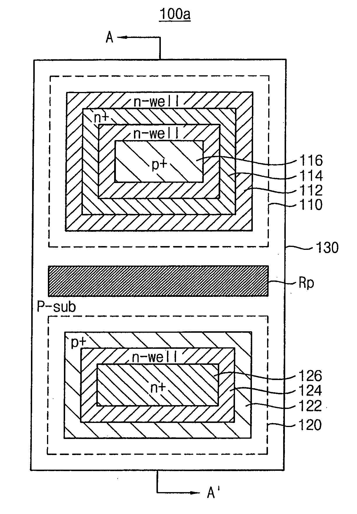
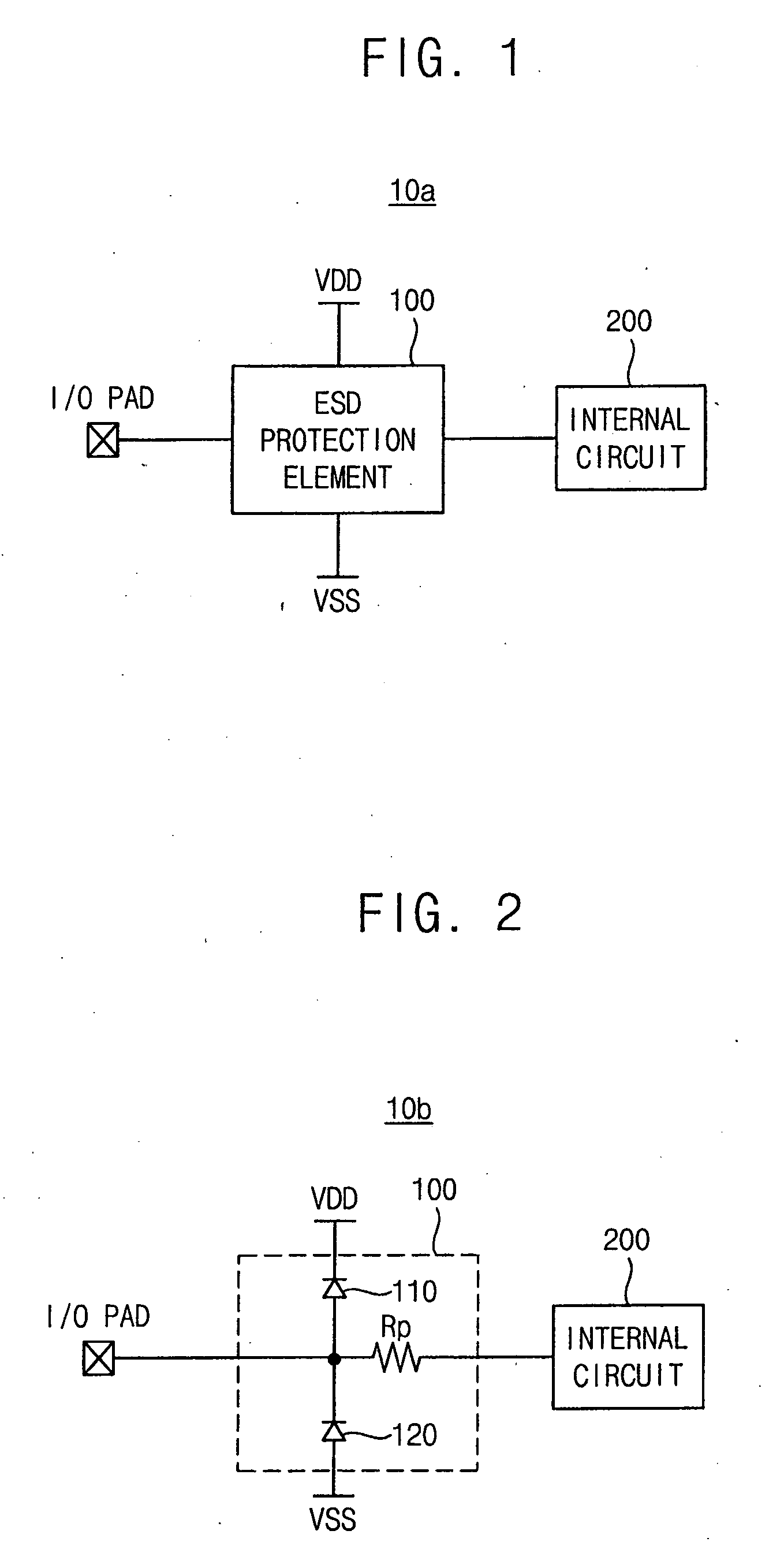
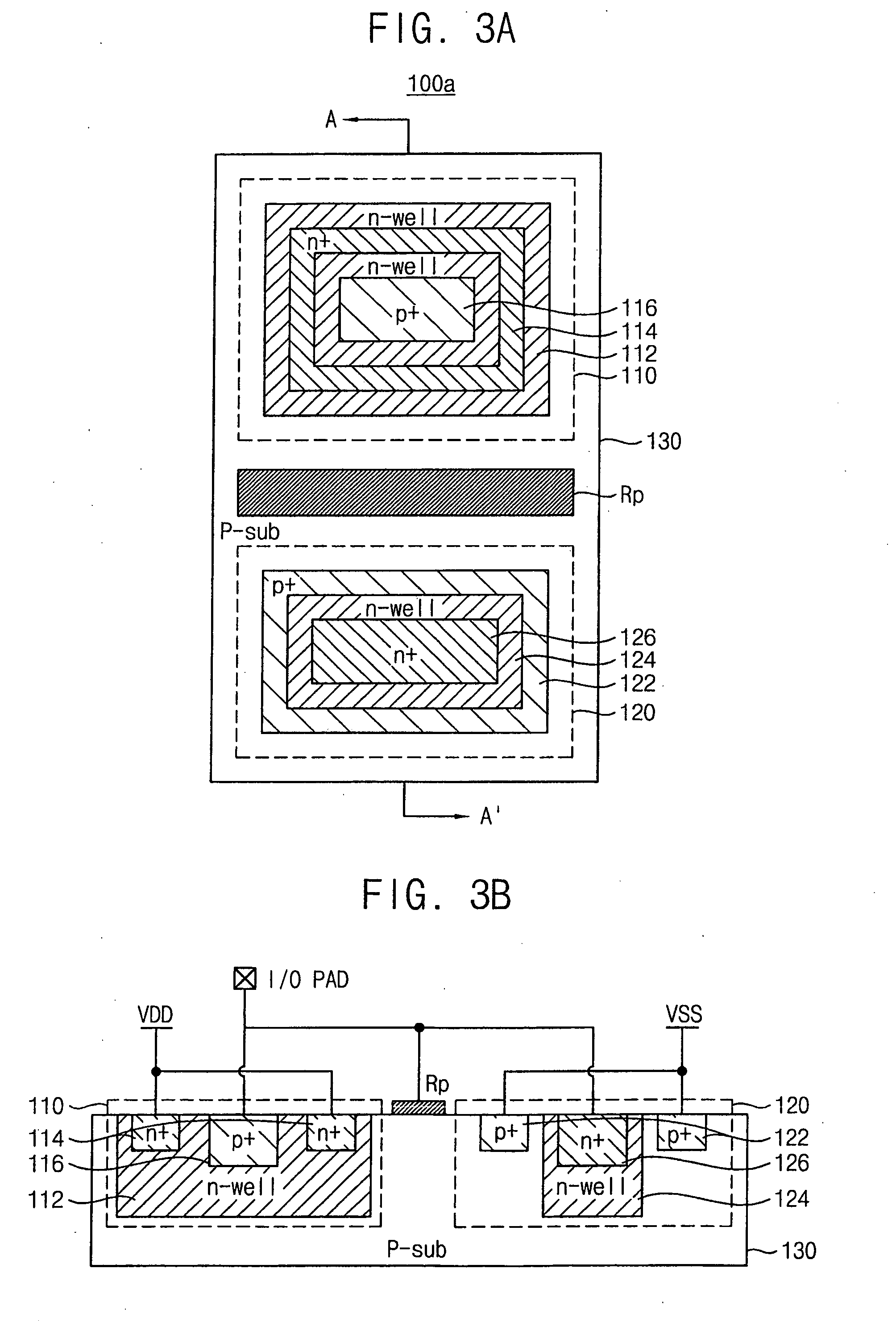
[0042]Embodiments of the inventive concept now will be described more fully with reference to the accompanying drawings, in which embodiments in accordance with aspects of the inventive concept are shown. The present inventive concept may, however, be embodied in many different forms and should not be construed as limited to the embodiments set forth herein. Like reference numerals refer to like elements throughout this application.

[0043]It will be understood that, although the terms first, second, etc. may be used herein to describe various elements, these elements should not be limited by these terms. These terms are used to distinguish one element from another. For example, a first element could be termed a second element, and, similarly, a second element could be termed a first element, without departing from the scope of the inventive concept. As used herein, the term “and / or” includes any and all combinations of one or more of the associated listed items.

[0044]It will be under...


PUM


Abstract

An electrostatic discharge (ESD) protection element includes a first diode, a second diode, and a poly resistor. The first diode is connected between a first voltage and an input/output (I/O) pad. The second diode is connected between the I/O pad and a second voltage. The poly resistor is formed on the second diode.

Description

CROSS-REFERENCE TO RELATED APPLICATIONS[0001]This application claims priority under 35 USC §119 to Korean Patent Application No. 10-2009-0016348, filed on Feb. 26, 2009 in the Korean Intellectual Property Office (KIPO), the disclosure of which is incorporated herein in its entirety by reference.BACKGROUND[0002]1. Technical Field[0003]Example embodiments relate to an electrostatic discharge protection circuit and more particularly to an electrostatic discharge protection element in a semiconductor memory device.[0004]2. Description of the Related Art[0005]An electrostatic discharge (ESD) is a momentary electric current which flows between two objects having different electrical potentials caused by a direct contact or induced by an electrostatic field.[0006]Semiconductor memory devices may include ESD protection circuits between an input / output (I / O) pad and an internal circuit to prevent the ESD from damaging isolation layers and channel regions formed in the internal circuit.[0007]...

Claims


Application Information

Patent Timeline
Patent Type & Authority Applications(United States)
IPC IPC(8): H02H9/04H01L27/06
CPCH01L27/0676H01L27/0288H01L27/04
Inventor KIM, SUK-JINKIM, HAN-GUKO, JAE-HYOKBAN, HYO-CHEOLKO, MIN-CHANGJEON, KYOUNG-KI
Owner SAMSUNG ELECTRONICS CO LTD
Why Eureka
Try Eureka