Method of manufacturing organic electroluminescent device

a manufacturing method and electroluminescent technology, applied in the direction of organic semiconductor devices, semiconductor devices, coatings, etc., can solve the problems of low low operating voltage, and reduced light-emitting efficiency and lifetime of organic electroluminescent devices, so as to maintain electron injection efficiency, improve light-emitting efficiency, and work function high

Inactive Publication Date: 2010-08-26
INNOLUX CORP
View PDF14 Cites 7 Cited by
  • Summary
  • Abstract
  • Description
  • Claims
  • Application Information

AI Technical Summary

Benefits of technology

[0012]The doped buffer layer provides a function of protecting the thin metal layer and the underlying and maintains the electron injection efficiency even when the materials of the transparent electrode have a high work function. Therefore, an embodiment of the present invention provides a top-emission or a dual emission OLED having the organic electroluminescent devices, which has preferable light-emitting efficiency and a long lifetime.

Problems solved by technology

The damage would result in lower light-emitting efficiency and lifetime of the organic electroluminescent devices.
Therefore, one of the disadvantages of the above-mentioned disclose is that the light-emitting efficiency and lifetime of the organic electroluminescent devices are decreased.
In addition, the utilization of CuPc near the cathode leads to high operating voltages.
Furthermore, the evaporation temperature of CuPc is much higher than other organic materials and it is hard to clean CuPc materials so that the evaporation chamber is easily contaminated during forming the CuPc layer.
Accordingly, the TOLED 200 with CuPc material is not suitable for applying to mass production.
Accordingly, to provide a method of manufacturing an organic electroluminescent device with preferable light-emitting efficiency, easily fabricated in mass production, is still an important issue for manufactures.

Method used


Image

  • Method of manufacturing organic electroluminescent device
  • Method of manufacturing organic electroluminescent device
  • Method of manufacturing organic electroluminescent device

Examples


Embodiment Construction

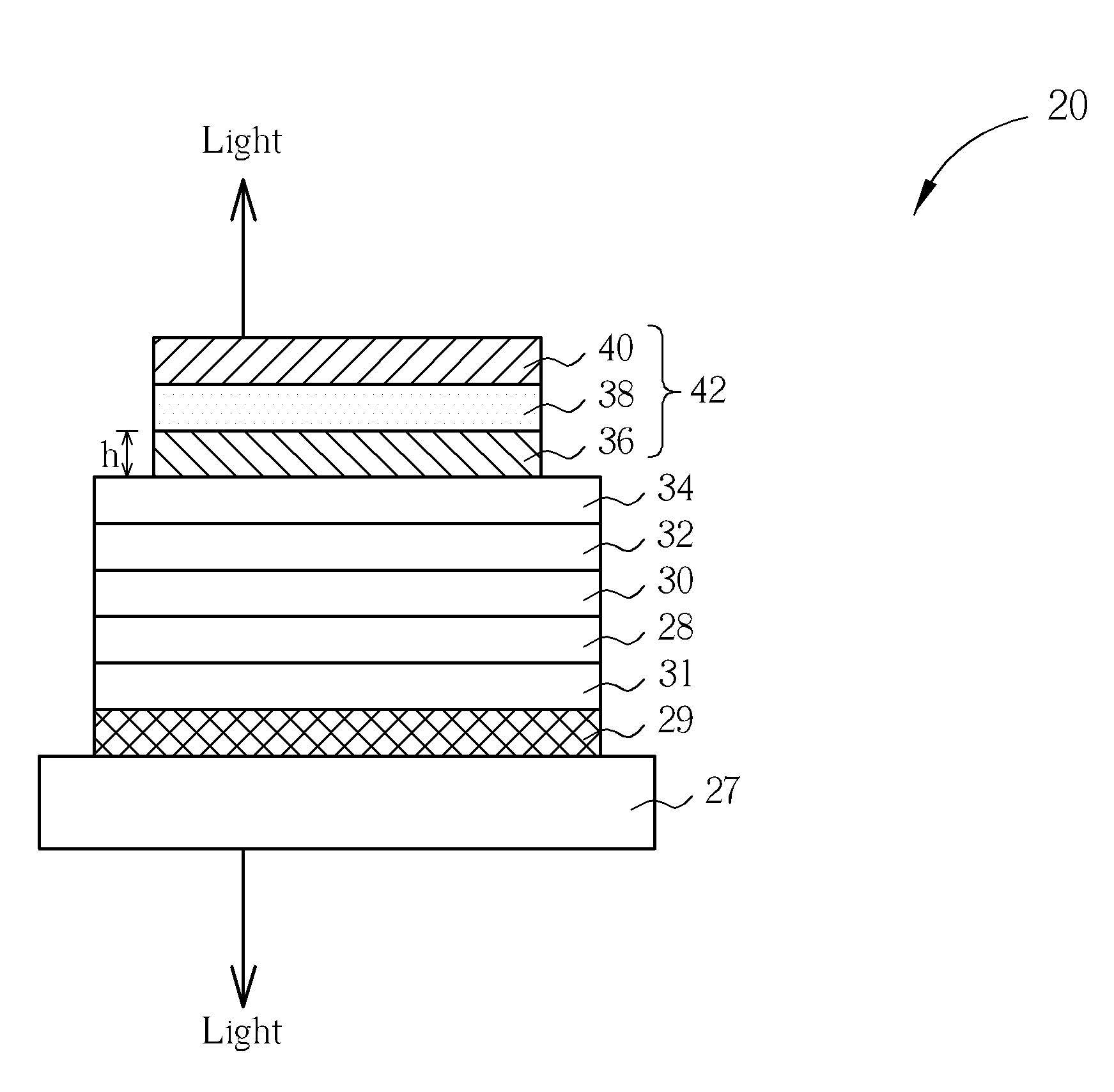
[0018]FIG. 3 is a top view of an electronic device for displaying images according to an embodiment of the present invention. As shown in FIG. 3, the electronic device 1 that comprises an input device 15 and an organic electroluminescent display (OLED) 10. The electronic device 1 may be a portable device such as a PDA, notebook computer, tablet computer, cellular phone, or a display monitor device, etc. Input device 15 can be coupled to the OLED 10. The input device 15 can include a processor or the like to provide image data to a control circuit 14 to render images. The OLED 10 comprises a display area 12 including a matrix composed of a plurality of data lines 22 (such as D1, D2, and D3) and scan lines 24 (such as S1, S2, and S3). The display area 12 also comprises a plurality of sub-pixel circuits 26, wherein each sub-pixel circuit 26 has at least one thin film transistor (TFT) and an organic electroluminescent device 20 at each intersection of a data line 22 and a scan line 24. ...


PUM

PropertyMeasurementUnit
thicknessaaaaaaaaaa
thicknessaaaaaaaaaa
thicknessaaaaaaaaaa

Abstract

A method of manufacturing an organic electroluminescent device is provided. First, a substrate and an anode on the substrate are provided, and then, an organic electroluminescent material layer is formed on the anode. Next, a multi-layer transparent cathode is formed on the organic electroluminescent layer. The step of forming the multi-layer transparent cathode comprises performing a co-evaporation process to form a doped buffer layer comprising electron transport materials and dopant so as to distribute the dopant uniformly in the electron transport materials.

Description

CROSS REFERENCE TO RELATED APPLICATIONS[0001]This is a continuation-in-part of U.S. application Ser. No. 11 / 402,442, which was filed on Apr. 12, 2006 and is included herein by reference.BACKGROUND OF THE INVENTION[0002]1. Field of the Invention[0003]The invention relates to a method of manufacturing an organic electroluminescent device, and more particularly, to a method of manufacturing an organic electroluminescent device with a buffer layer in the cathode.[0004]2. Description of the Prior Art[0005]In various types of flat panel displays, since an organic electroluminescent display (OLED) has many beneficial characteristics, such as having a spontaneous light source, a wide viewing angle, fast response time, full-color, simpler structure, and power savings, the OLED has been used extensively in small and medium scale portable display fields.[0006]An OLED is composed of many organic electroluminescent devices that comprise organic electroluminescent materials. U.S. Pat. No. 6,548,9...

Claims


Application Information

Patent Timeline
Patent Type & Authority Applications(United States)
IPC IPC(8): B05D5/12
CPCH01L51/0081H01L2251/5323H01L51/5234H10K85/324H10K50/828H10K2102/3031
Inventor HUANG, CHI-HSIENYEH, PEI-HSUN
Owner INNOLUX CORP
Why Eureka
Try Eureka