Manufacturing method of substrate structure

a manufacturing method and substrate technology, applied in the direction of printed circuit manufacturing, conductive pattern formation, printed element electric connection formation, etc., can solve the problems of insufficient space and skip plating, and achieve the effect of achieving a preferable process yield ra

Inactive Publication Date: 2015-03-10
SUBTRON TECH
View PDF10 Cites 5 Cited by
  • Summary
  • Abstract
  • Description
  • Claims
  • Application Information

AI Technical Summary

Benefits of technology

[0007]The invention provides a method for manufacturing a substrate structure, a first gold layer, a nickel layer and a second gold layer are successively formed on the patterned copper layers thereof, said method not only provides a more preferable process yield rate, but also maintains integrity of the microwaves communication signals.
[0016]In view of above, the substrate structure of the invention is manufactured by forming the first gold layer, the nickel layer and the second gold layer successively on the patterned copper layers. In comparing with the method for forming the nickel layer, the palladium layer and the gold layer successively on a patterned copper layer of the conventional substrate structure, the manufacturing method of the substrate structure of the invention not only provides a more preferable process yield rate, but also maintains integrity of the microwaves communication signals.

Problems solved by technology

Furthermore, since the nickel layer is formed by chemical plating (i.e. nickel-plating with a reduction method), problems such as unstable electroplating solution and incomplete coverage of the nickel layer may occur, thereby causing a skip plating problem in the following chemical plating process for palladium-plating.
However, the nickel layer with such thickness may cause a problem of insufficient space when being used in the products with smaller circuit gaps.

Method used


Image

  • Manufacturing method of substrate structure
  • Manufacturing method of substrate structure
  • Manufacturing method of substrate structure

Examples


Embodiment Construction

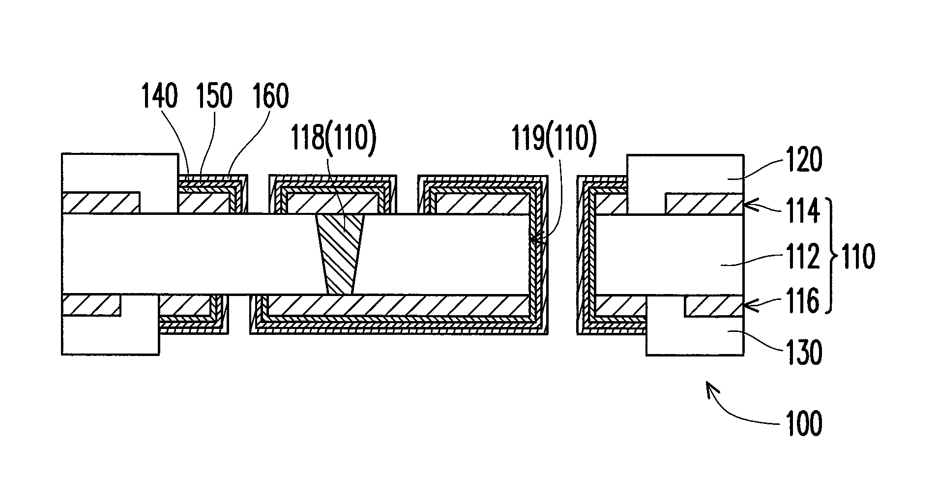
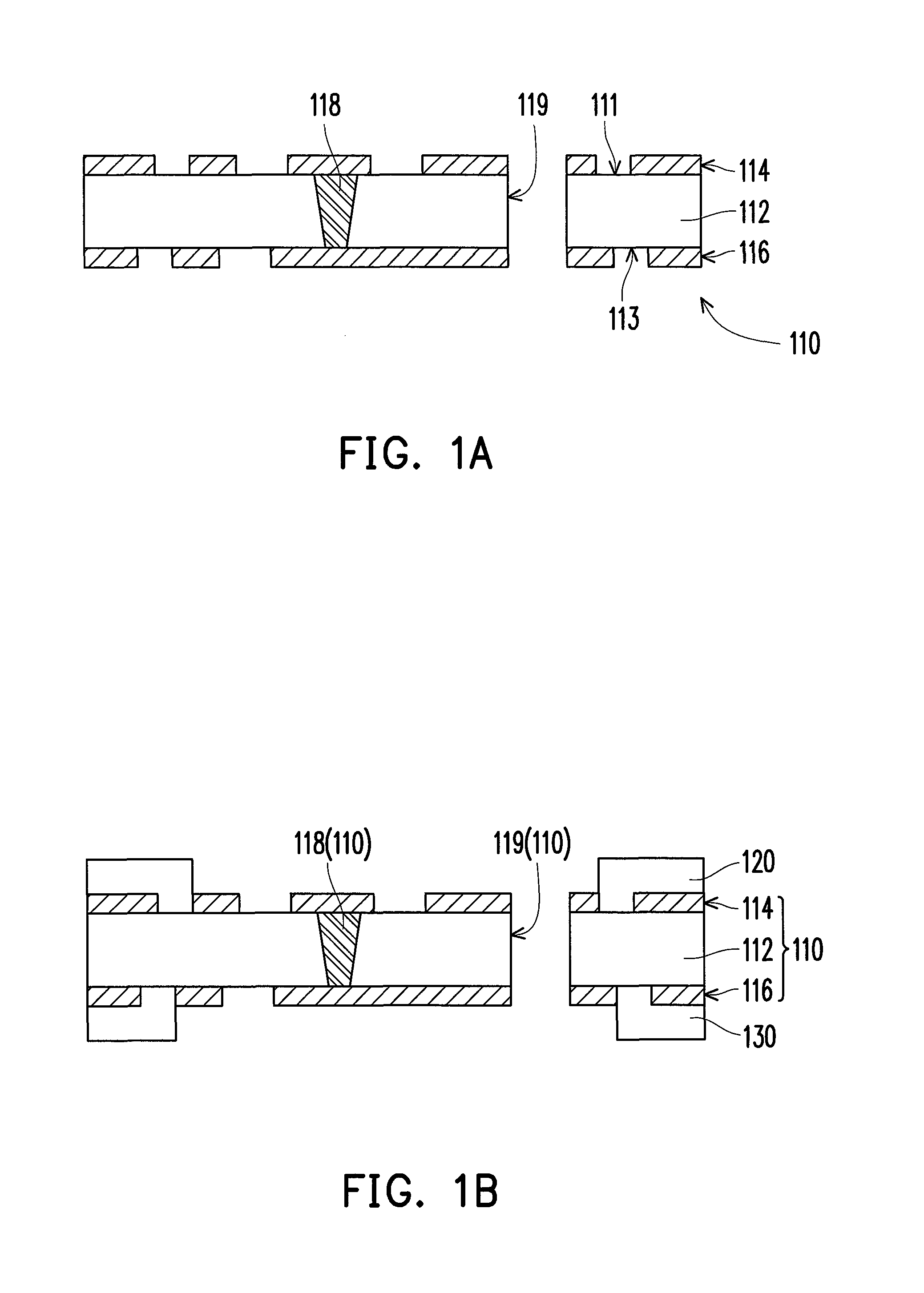
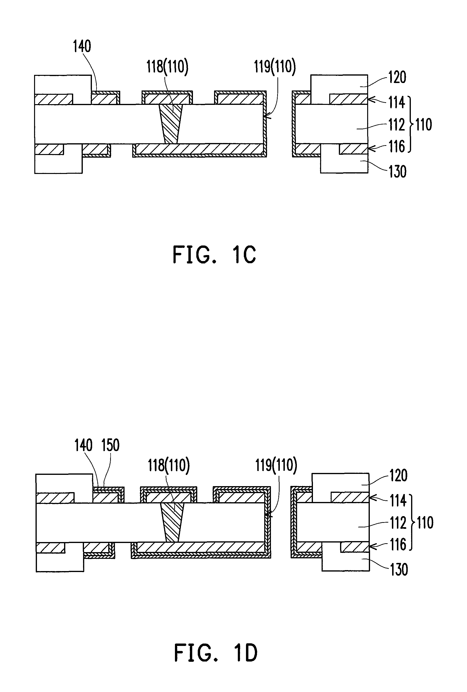
[0019]FIG. 1A to FIG. 1E are schematic cross-sectional views illustrating a manufacturing method of a substrate structure according to an embodiment of the invention. Referring to FIG. 1A, according to the manufacturing method of a substrate structure in this embodiment, a base material 110 is provided. More specifically, the base material 110 has a core layer 112, a first patterned copper layer 114, a second patterned copper layer 116 and at least one conductive via 118 (only one conductive via is schematically illustrated in FIG. 1A). The core layer 112 has a first surface 111 and a second surface 113 opposite to each other. The first patterned copper layer 114 and the second patterned copper layer 116 are respectively located on the first surface 111 and the second surface 113. The conductive via 118 passes through the core layer 112 and connects the first patterned copper layer 114 and the second patterned copper layer 116. In addition, the base material 110 according to the pre...


PUM

PropertyMeasurementUnit
thicknessaaaaaaaaaa
thicknessaaaaaaaaaa
thicknessaaaaaaaaaa

Abstract

A manufacturing method of substrate structure is provided. A base material having a core layer, a first patterned copper layer, a second patterned copper layer and at least one conductive via is provided. The first and second patterned copper layers are respectively located on a first surface and a second surface of the core layer. The conductive via passes through the core layer and connects the first and second patterned copper layers. A first and a second solder mask layers are respectively formed on the first and second surfaces. Portions of the first and second patterned copper layers are exposed by the first and second solder mask layers, respectively. A first gold layer is formed on the first and second patterned copper layers exposed by the first and second solder mask layers. A nickel layer and a second gold layer are successively formed on the first gold layer.

Description

CROSS-REFERENCE TO RELATED APPLICATION[0001]This application claims the priority benefit of Taiwan application serial no. 101123724, filed on Jul. 2, 2012. The entirety of the above-mentioned patent application is hereby incorporated by reference herein and made a part of this specification.BACKGROUND OF THE INVENTION[0002]1. Field of the Invention[0003]The invention relates to a manufacturing method of a substrate structure, and more particularly to a manufacturing method of a substrate structure having a more preferable process yield rate.[0004]2. Description of Related Art[0005]Packaging of integrated circuit is an important step in the back-end process for manufacturing a semiconductor, the purpose thereof is to protect each chip after manufacturing process and to electrically connect the pads of the chip and printed circuit board (PCBs). The PCBs and chip carrier substrates have multiple solder joints, a process of surface finishing or metallization need to be performed on a co...

Claims


Application Information

Patent Timeline
Patent Type & Authority Patents(United States)
IPC IPC(8): H05K3/20
CPCH01L21/486H05K3/244H05K3/42H05K3/428Y10T29/49128Y10T29/49146Y10T29/49155Y10T29/49165Y10T29/49169
Inventor CHEN, CHING-SHENG
Owner SUBTRON TECH
Why Eureka
Try Eureka