Printed wiring board, printed IC board having the printed wiring board, and method of manufacturing the same

a technology of printed wiring boards and printed ic boards, which is applied in the direction of printed element electric connection formation, printed circuit non-printed electric components association, etc., can solve the problems of preventing a suitable bonding between a bare ic chip and bump parts, reducing the reliability of printed ic boards, etc., and achieves the effect of easy assembly of the reinforcing member

Inactive Publication Date: 2010-09-09
DENSO CORP
View PDF9 Cites 8 Cited by
  • Summary
  • Abstract
  • Description
  • Claims
  • Application Information

AI Technical Summary

Benefits of technology

[0019]According to the method of manufacturing the printed IC board, it is possible to easily lay the reinforci...

Problems solved by technology

This decreases the reliability of the printed IC board because the insulation material contained in the printed wiring board placed on the heat stage unit disperses ultrasonic waves and distri...

Method used


Image

  • Printed wiring board, printed IC board having the printed wiring board, and method of manufacturing the same
  • Printed wiring board, printed IC board having the printed wiring board, and method of manufacturing the same
  • Printed wiring board, printed IC board having the printed wiring board, and method of manufacturing the same

Examples


first embodiment

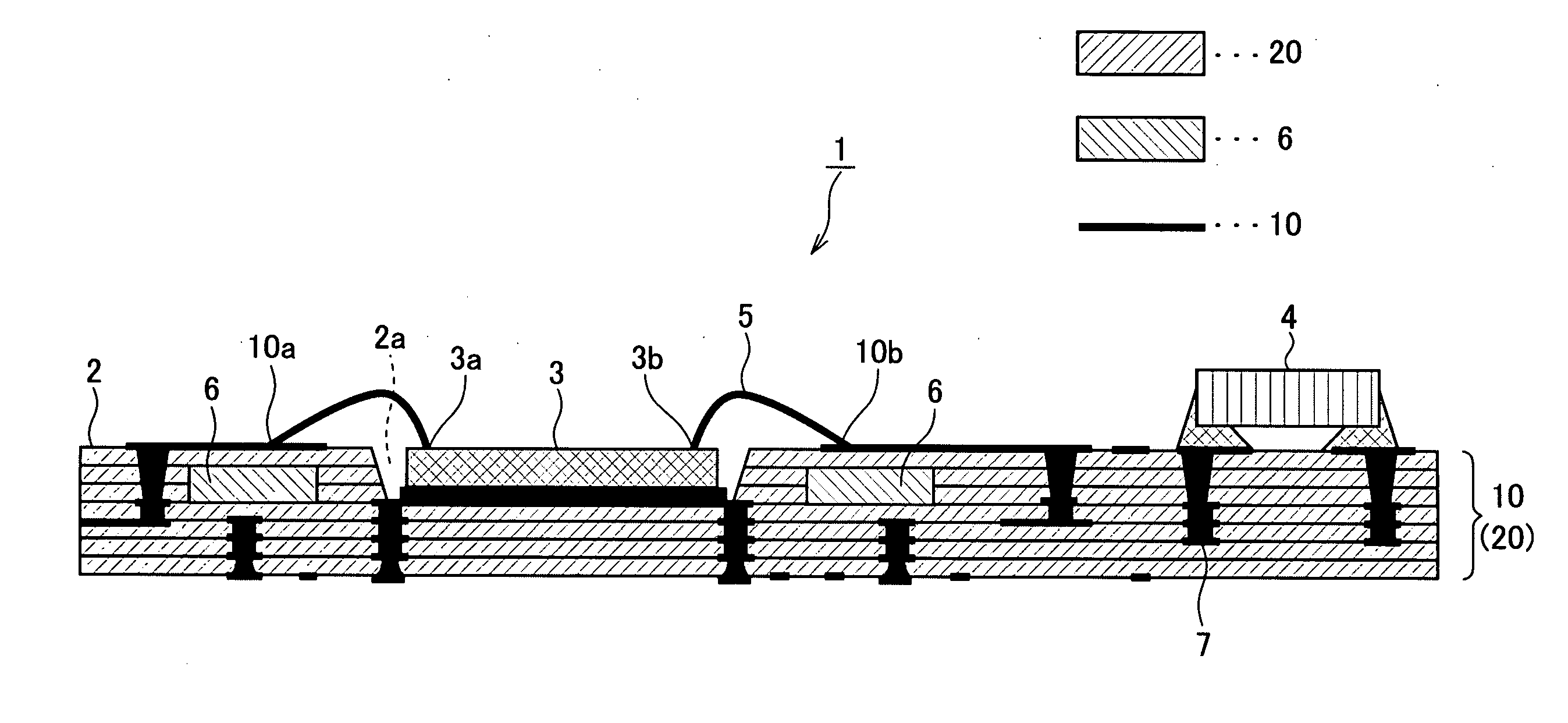
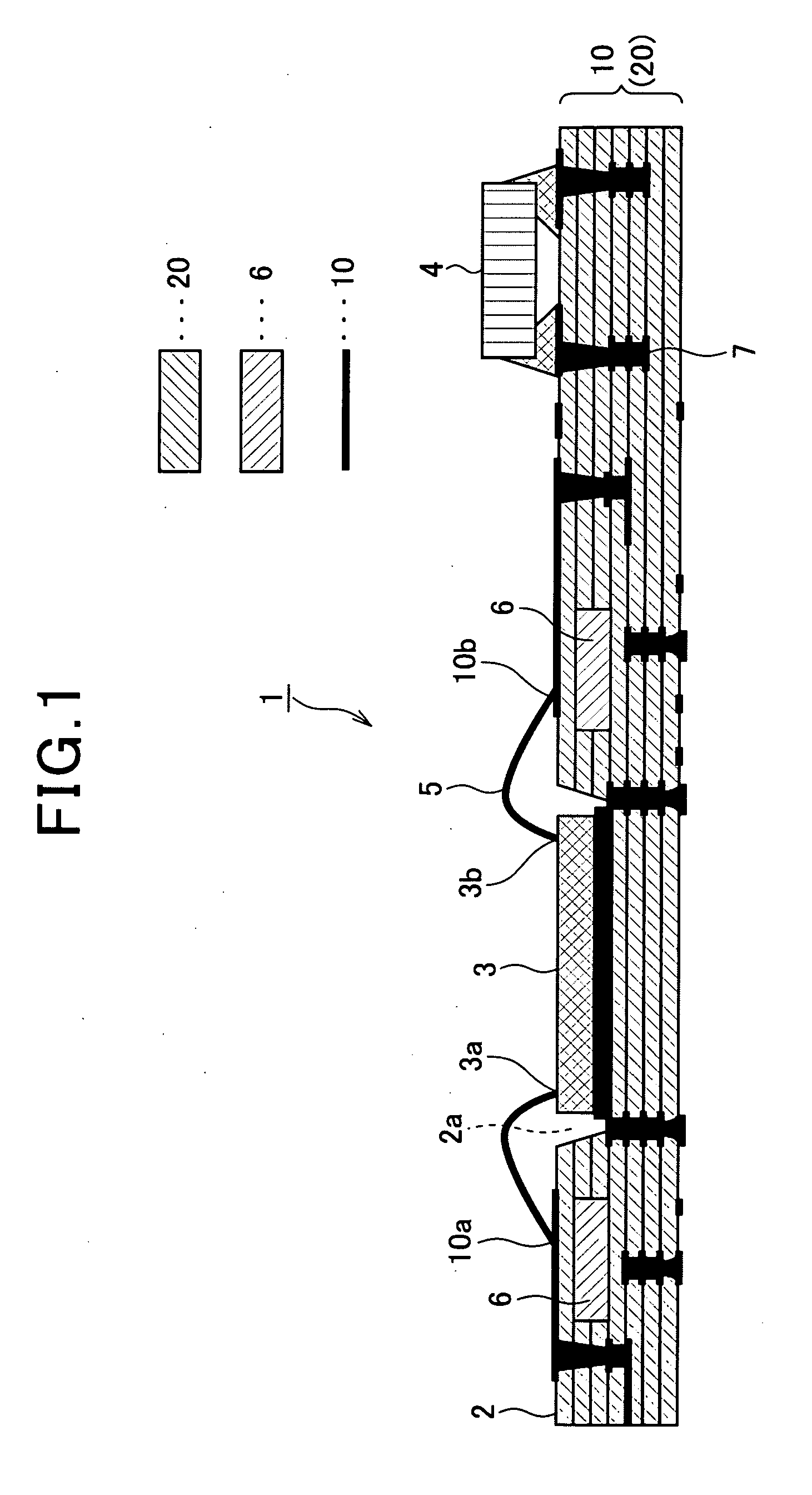
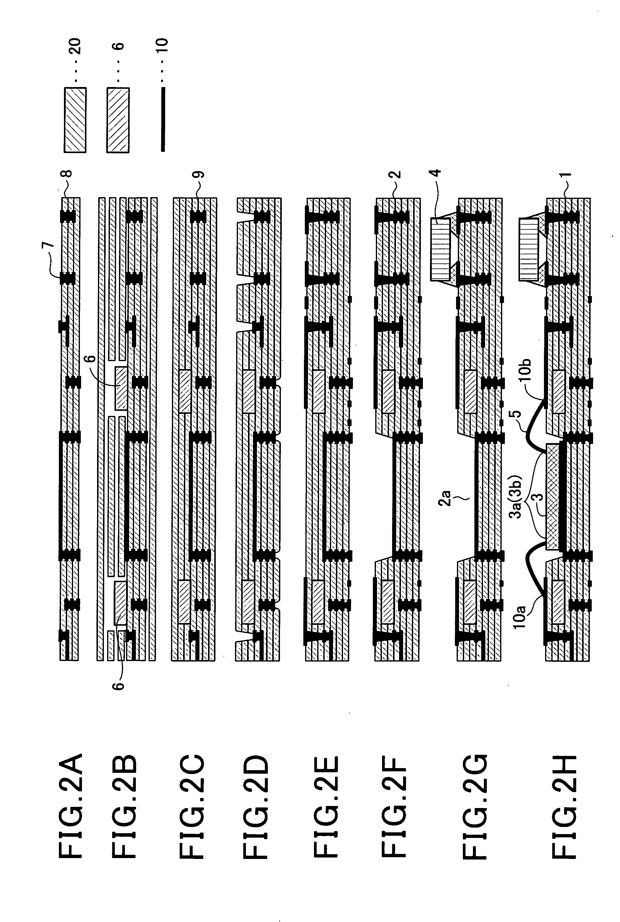
[0029]A description will be given of a printed IC board (or a printed IC assembly) according to the first embodiment of the present invention with reference to FIG. 1 to FIGS. 2A-2H.

[0030]FIG. 1 is a view showing a configuration of the printed IC board 1 according to the first embodiment of the present invention. FIG. 2A to FIG. 2H are views showing main steps of manufacturing the printed IC board 1 according to the first embodiment of the present invention.

[0031]As shown in FIG. 1, the printed IC board 1 is composed mainly of a multilayer printed wiring board 2, one or more bare IC chips 3 (by the way, FIG. 1 only shows a single bare IC chip 3 for brevity), and chip components 4 such as capacitances and resistances. The multilayer printed wiring board 2 has a multilayered structure in which a plurality of printed wiring patterns is stacked to make a lamination structure, where the printed wiring pattern is made of a copper thin film. The bare IC chip 3 is made of semiconductor such...

second embodiment

[0048]A description will be given of the printed IC board 1-1 according to the second embodiment of the present invention with reference to FIGS. 3A to 3C, and FIGS. 4A to 4E.

[0049]FIG. 3A, FIG. 3B, and FIG. 3C are views showing a configuration of the printed IC board 1-1 according to the second embodiment of the present invention. FIG. 4A to FIG. 4E are views showing main steps of producing the printed IC board 1-1 according to the second embodiment of the present invention.

[0050]As shown in FIG. 3A, FIG. 3B, and FIG. 3C, the printed IC board 1-1 has a multilayer printed wiring board 2-1 which is different in structure from the multilayer printed wiring board 2 in the printed IC board 1 according to the first embodiment. The following description will explain different components from the components of the printed IC board 1 according to the first embodiment, and not explain the same components between the first and second embodiments for brevity.

[0051]The multilayer printed wiring...

third embodiment

[0060]A description will be given of the printed IC board 1-2 according to the third embodiment of the present invention with reference to FIG. 5 and FIGS. 6A to 6G.

[0061]FIG. 5 is a view showing a configuration of the printed IC board 1-2 according to the third embodiment of the present invention. FIG. 6A to FIG. 6G are views showing main steps of producing the printed IC board 1-2 according to the third embodiment of the present invention.

[0062]As shown in FIG. 5, the printed IC board 1-2 according to the third embodiment has a multilayer printed wiring board 2-2 which is different in structure from the multilayer printed wiring board 2 in the printed IC board 1 according to the first embodiment, and also from the multilayer printed wiring board 2-1 in the printed IC board 1-1 according to the second embodiment.

[0063]Because the printed IC board 1-2 according to the third embodiment is different in connection structure between the bare IC chip and the multilayer printed wiring boa...


PUM

PropertyMeasurementUnit
Thicknessaaaaaaaaaa
Stiffnessaaaaaaaaaa
Expansion enthalpyaaaaaaaaaa

Abstract

A printed IC board has a multilayer printed wiring board and one or more bare IC chips. The multilayer printed wiring board has insulation layers made of PTFE, and wiring patterns formed on the insulation layers which are stacked to make a lamination structure. Electrode parts as parts of the wiring patterns are electrically connected to the bare IC chip. A copper member which serves as a reinforcing member is laid in a region formed in the insulation layers other than a first insulation layer. the region is formed directly below the electrode parts. The region is formed in a direction Z along a thickness of the stacked insulation layers. The region formed directly below the electrode parts in the insulation layers in the insulation layers other than the first insulation layer has a higher rigidity than the insulation layers.

Description

CROSS-REFERENCE TO RELATED APPLICATION[0001]This application is related to and claims priority from Japanese Patent Application No. 2009-55533 filed on Mar. 9, 2009, the contents of which are hereby incorporated by reference.BACKGROUND OF THE INVENTION[0002]1. Field of the Invention[0003]The present invention relates to a printed wiring board, a printed integrated circuit (IC) board (or a printed IC assembly) composed of one or more bare IC chips and the printed wiring board having insulation layers and printed wiring patterns, and a method of manufacturing the printed wiring board and the printed IC board.[0004]2. Description of the Related Art[0005]Various types of a printed IC board (or printed IC assembly) composed of a printed wiring board are well known. For example, a printed wiring board has an insulation layer and a printed wiring pattern made of conductive wires such as copper wires. The insulation layer is made of insulation material which is selected according to its app...

Claims


Application Information

Patent Timeline
IPC IPC(8): H05K1/18H05K3/10H05K3/40H05K3/46
CPCH01L23/13H01L23/49822H01L23/5389H01L24/16H01L24/45H01L24/48H01L24/49H01L2224/16H01L2224/32225H01L2224/45144H01L2224/45147H01L2224/48091H01L2224/48227H01L2224/49175H01L2224/49433H01L2224/73265H01L2224/85205H01L2224/92H01L2224/92247H01L2924/01004H01L2924/01014H01L2924/01015H01L2924/01078H01L2924/01079H01L2924/14H01L2924/15153H01L2924/15157H01L2924/1517H01L2924/19041H01L2924/19043H01L2924/19105H01L2924/30105H01L2924/3011H01L2924/3511H05K1/0271H05K1/034H05K1/181H05K1/183H05K3/4632H05K2201/015H05K2201/09781H05K2201/10674H05K2201/2009H05K2203/049H01L2924/01019H01L2924/01013H01L2924/01047Y10T29/49155Y10T29/49165Y10T29/4913H01L2924/00014H01L2924/00H01L2924/00012H01L23/49894H01L24/73H01L2224/13144H01L2224/13147H01L2224/2919H01L2224/2929H01L2224/81205H01L2924/00011H01L2924/10253H01L2924/30111H01L2224/0401H01L2924/0665H01L2924/0715
Inventor KOUYA, TAKUYA
Owner DENSO CORP
Why Eureka
Try Eureka