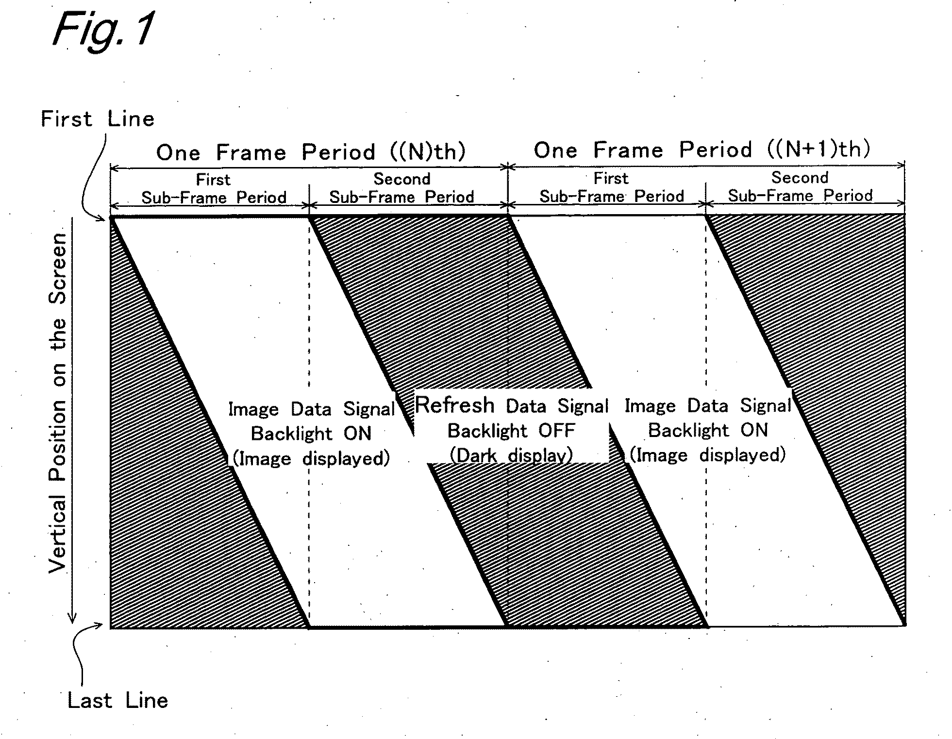
[0050]According to the first, second or eleventh aspect of the present invention, each pixel formation portion is supplied with a pixel voltage based on an entered
image signal in the first sub-frame period whereas each pixel formation portion is supplied with a refresh voltage based on the entered
image signal in the second sub-frame period, in each frame period. Also, the pixel formation portions which are supplied with a pixel voltage in the first sub-frame period receive light from the lighting device until refresh voltage is supplied in the second sub-frame period. Thereafter, however, light from the lighting device is not supplied until a pixel voltage is supplied in the first sub-frame period of the next frame period. Therefore, it is possible to prevent screen burn caused by prolonged display of the same
image based on an entered image while keeping the image always on display. Further, viewers do not perceive unnecessary display made by the refresh voltage.
[0051]According to the third aspect of the present invention, a liquid
crystal display device includes a plurality of pixel formation portions disposed in a
matrix pattern. In each frame period, each pixel formation portion is supplied with a pixel voltage based on an entered image in the first sub-frame period upon selection by the scanning line, whereas each pixel formation portion is supplied with a refresh voltage in the second sub-frame period upon selection by the scanning line. Also, the matrix of the pixel formation portions is divided into units each consisting of a predetermined number of lines, and ON / OFF control is provided on the light sources for each unit upon selection by the scanning signal line. Thus, the pixel formation portions which are supplied with a pixel voltage in the first sub-frame period receive light from the lighting device until a refresh voltage is supplied in the second sub-frame period. Thereafter, however, light from the lighting device is not supplied until a pixel voltage is supplied in the first sub-frame period of the next frame period. The operations described above provide the same advantages as offered by the first aspect.
[0052]According to the fourth aspect of the present invention, an
active matrix liquid
crystal display device includes a plurality of pixel formation portions disposed in a
matrix pattern. In each frame period, each pixel formation portion is supplied with a pixel voltage based on an entered image in the first sub-frame period upon selection by the scanning line, whereas each pixel formation portion is supplied with a refresh voltage in the second sub-frame period upon selection by the scanning line. Also, the matrix of the pixel formation portions is divided into units each consisting of a predetermined number of lines, and ON / OFF control is provided on the light sources of the lighting device for each unit in response to selection by the scanning signal line. With this arrangement, those pixel formation portions which are supplied with a pixel voltage in the first sub-frame period hold the pixel voltage and receive light from the lighting device until a refresh voltage is supplied in the second sub-frame period. Thereafter, however, the refresh voltage is held without lighting from the lighting device until a pixel voltage is supplied in the first sub-frame period of the next frame period. The operations described above provide the same advantages as offered by the first aspect.
[0053]According to the fifth or the thirteenth aspect of the present invention, the length of the first sub-frame period is substantially equal to the length of the second sub-frame period. This makes it possible to substantially equalize the length of period in which the liquid crystal is affected by the pixel voltage based on the entered
image signal and the length of period in which the liquid crystal is affected by the refresh voltage, leading to substantially equalized
moving speed of the ionic impurities in the liquid crystal and a substantially constant
time average of the state of tilt of the liquid crystal molecules regardless of tone display levels. This arrangement effectively suppresses single-image prolonged-display screen burn.
[0054]According to the sixth or the fourteenth aspect of the present invention, the first tone value and the second tone value which are indicated respectively by the pixel voltage and the refresh voltage supplied to each pixel formation portion in each frame period have a
negative correlation with each other. This makes it possible to supply each pixel formation portion with voltages averaging to a substantially the same tone value, and thus makes it possible to suppress single-image prolonged-display screen burn.
[0055]According to the seventh or the fifteenth aspect of the present invention, there is a tone-reversal relationship between the first tone value indicated by the pixel voltage supplied in the first sub-frame period and the second tone value indicated by the refresh voltage supplied in the second sub-frame period in each frame period. With this arrangement, each pixel formation portion is supplied with voltages averaging to the same tone value in each frame period, and thus, it is possible to suppress single-image prolonged-display screen burn effectively.
[0056]According to the eighth aspect of the present invention, the polarity of the voltage applied to the liquid crystal layer in accordance with the pixel voltage or the refresh voltage supplied to each pixel formation portion is reversed for each frame period. This means that the voltage applied to the liquid crystal does not contain
direct current component, and thus it is possible to prevent screen burn caused by
residual charge.
[0057]According to the ninth aspect of the present invention, the voltage applied to the liquid crystal layer in accordance with the pixel voltage and the voltage applied to the liquid crystal layer in accordance with the refresh voltage are of the same polarity in the same frame period. Thus, screen burn caused by
residual charge can be prevented by reversing the polarity in each frame period.

