Systems and methods for manufacturing semiconductor device

a semiconductor device and manufacturing method technology, applied in the field of systems and methods for manufacturing semiconductor devices, can solve the problems of semiconductor device fault, mismatch between mask registration of the reticle used in consecutive processes, and difference between mask registration of the reticl

Inactive Publication Date: 2010-09-16
SAMSUNG ELECTRONICS CO LTD
View PDF4 Cites 2 Cited by
  • Summary
  • Abstract
  • Description
  • Claims
  • Application Information

AI Technical Summary

Problems solved by technology

Although a mask registration error may be within a management limit in one reticle, when reticles are manufactured in different facilities, a difference between mask registrations of the reticles may occur.
Also, when reticles are manufactured in the same facility, a mismatch between mask registrations of the reticles used in consecutive processes, e.g., prior and subsequent processes, may occur.
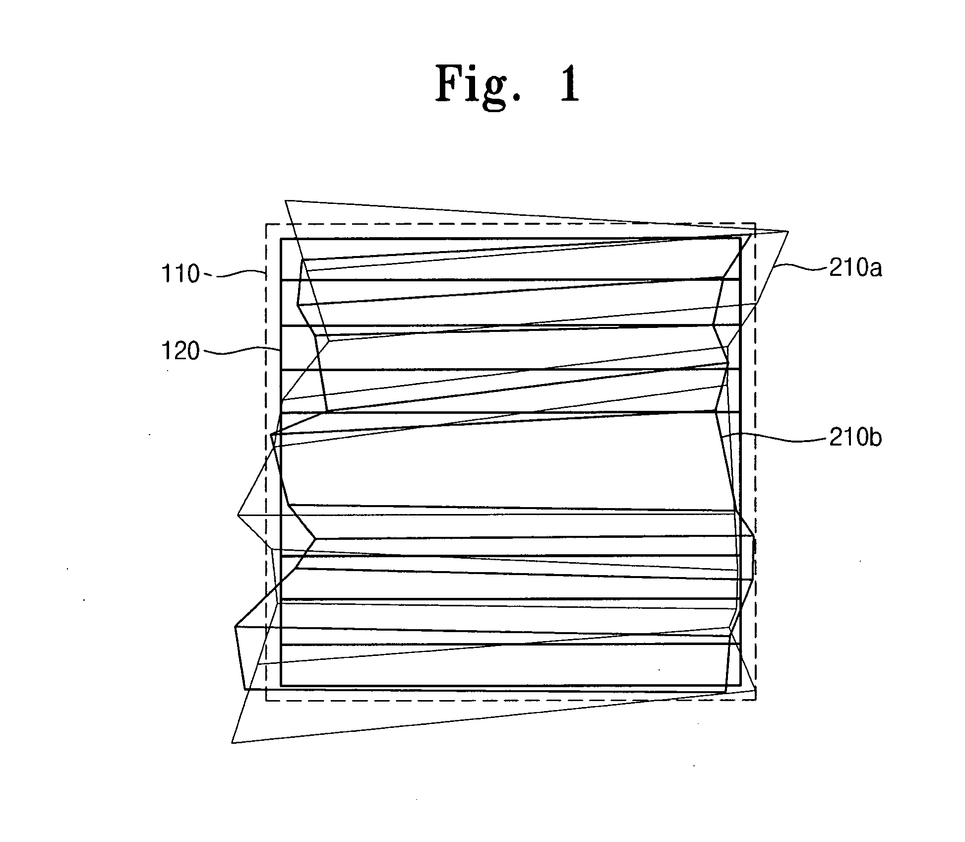
The mismatch between mask registrations of reticles may affect an interlayer overlay management on a wafer, thereby causing a misalignment between a real pattern and an overlay key measurement result on a wafer.
The misalignment between the real pattern and the overlay key measurement result on the wafer may cause a fault of a semiconductor device.

Method used


Image

  • Systems and methods for manufacturing semiconductor device
  • Systems and methods for manufacturing semiconductor device
  • Systems and methods for manufacturing semiconductor device

Examples


Embodiment Construction

[0020]Korean Patent Application No. 10-2009-0021738, filed on Mar. 13, 2009, in the Korean Intellectual Property Office, and entitled: “Systems and Methods for Manufacturing Semiconductor Device,” is incorporated by reference herein in its entirety.

[0021]Preferred embodiments will be described below in more detail with reference to the accompanying drawings. The embodiments may, however, be embodied in different forms and should not be constructed as limited to the embodiments set forth herein. Rather, these embodiments are provided so that this disclosure will be thorough and complete, and will fully convey the scope of the inventive concept to those skilled in the art. Like reference numerals refer to like elements throughout.

[0022]The terminology used herein is for the purpose of describing particular embodiments only and is not intended to be limiting of the invention. As used herein, the singular forms “a”, “an” and “the” are intended to include the plural forms as well, unless...


PUM


Abstract

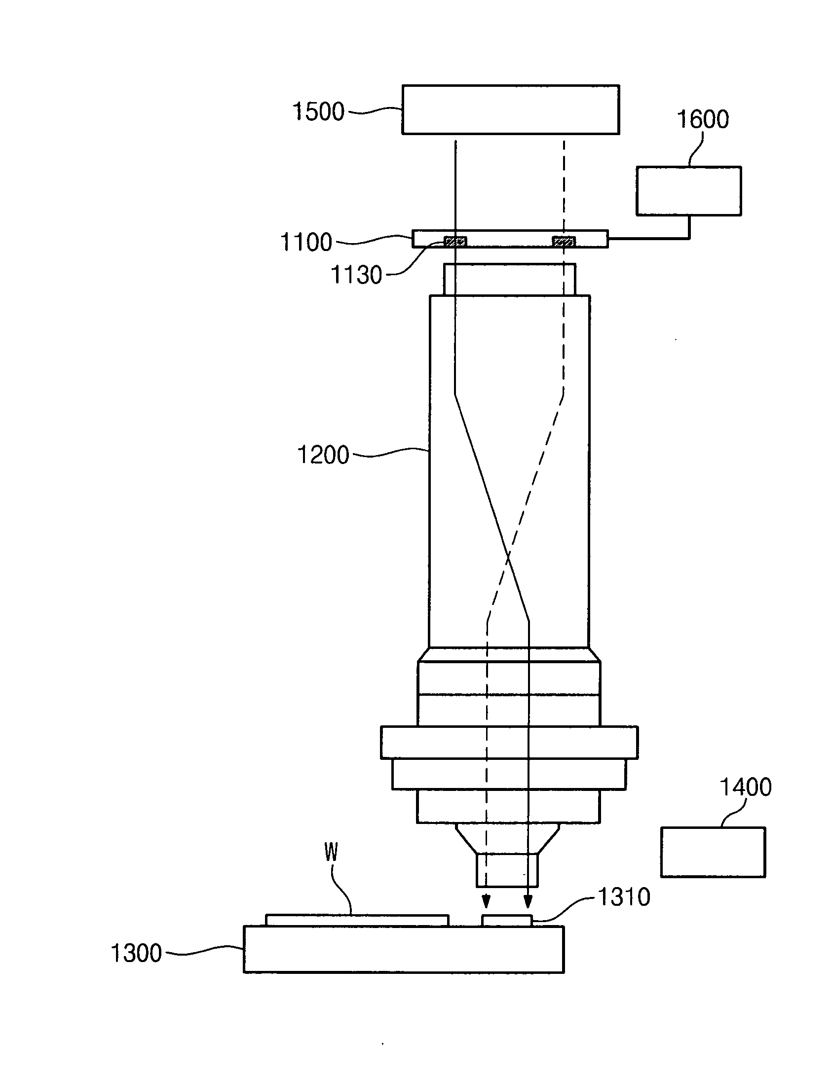
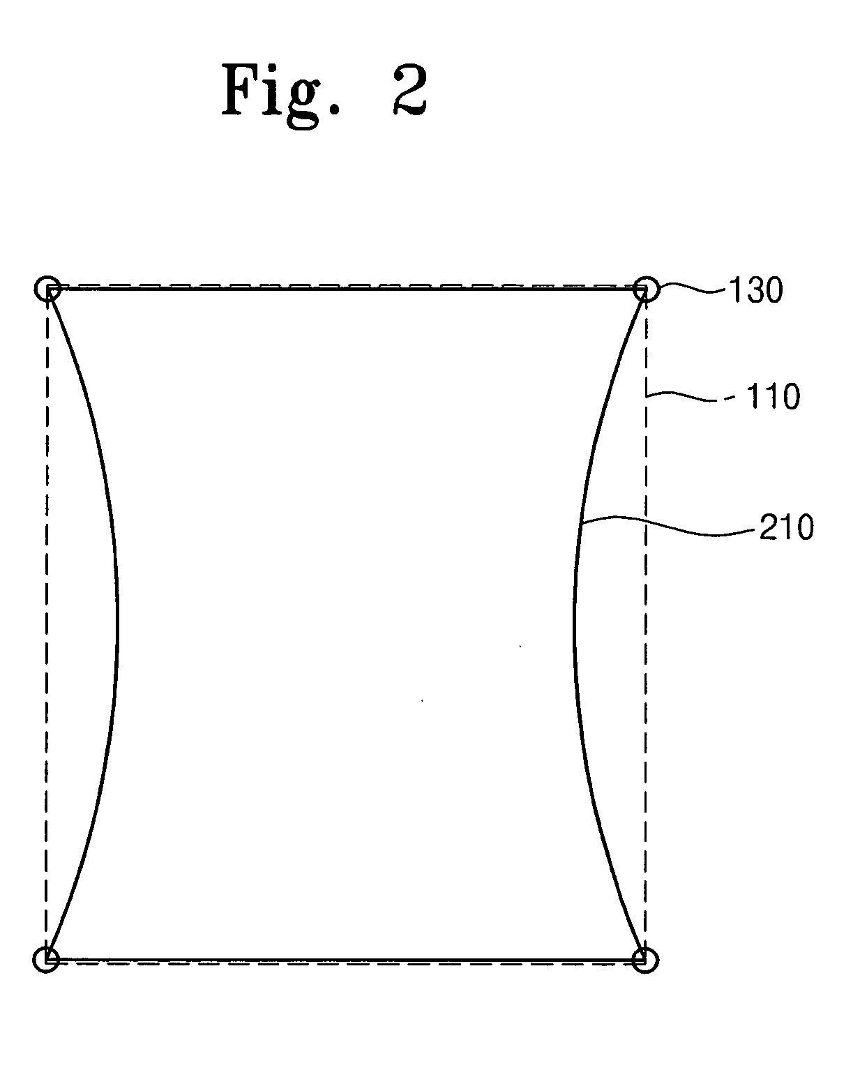
A method of manufacturing a semiconductor device includes preparing a reticle having at least three mask registration keys on respective four sides of a key field, aligning the reticle by irradiating light, after mounting the reticle on an exposure system, and measuring a mask registration including a non-linear term of the reticle from the mask registration keys using the irradiated light.

Description

BACKGROUND[0001]1. Field[0002]Example embodiments relate to systems and methods for manufacturing a semiconductor device, and more particularly, to systems and methods for manufacturing a semiconductor device using a reticle.[0003]2. Description of the Related Art[0004]Generally, an exposure facility is used in a photolithography process, which is one of the processes for manufacturing a semiconductor device. An exposure facility projects a circuit pattern corresponding to respective layers of an integrated circuit (IC) onto a wafer through a reticle, i.e., a mask, to form the circuit pattern on the wafer. The exposure facility may project a pattern image of the reticle onto a target region, i.e., a field region, of a wafer coated with a layer of photo sensitive material, e.g., photoresist, to form the reticle.[0005]Conventionally, a plurality of target regions, each of which is formed to be one semiconductor chip, may be formed to be adjacent to one another on a wafer. Pattern imag...

Claims


Application Information

Patent Timeline
Patent Type & Authority Applications(United States)
IPC IPC(8): G03B27/54
CPCG03F9/7007G03B27/54G03F7/70433G03F7/70516G03F9/7003G03F9/7065G03F9/7088
Inventor SHIN, HYESOOYOU, JIYONG
Owner SAMSUNG ELECTRONICS CO LTD
Why Eureka
Try Eureka