

Method for Manufacturing Photo Mask Using Fluorescence Layer
- Summary
- Abstract
- Description
- Claims
- Application Information
AI Technical Summary
Benefits of technology
Problems solved by technology
Method used
Image

Examples
Embodiment Construction
[0016]Hereinafter, a method for fabricating contacts in a semiconductor device in accordance with the invention is described in detail with reference to the accompanying drawings.
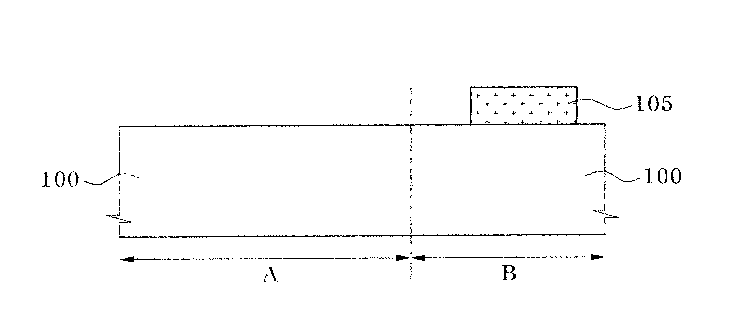
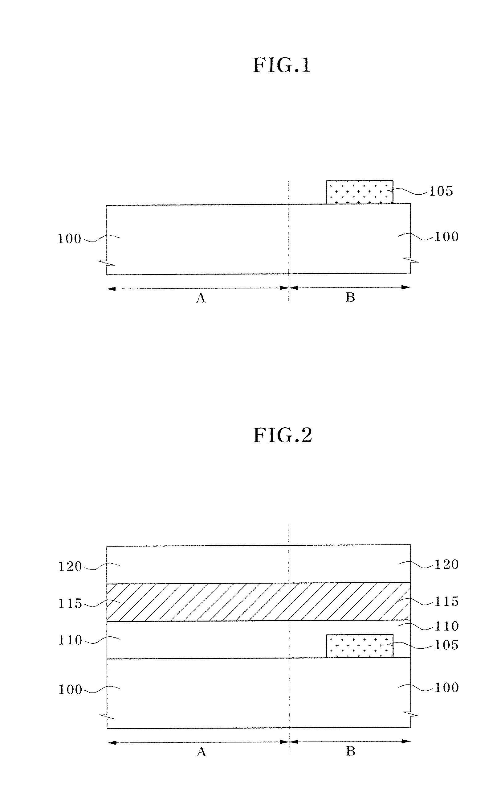
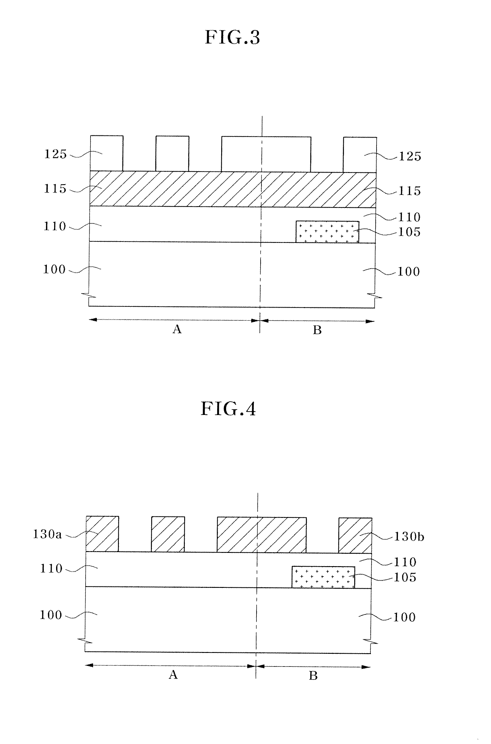
[0017]FIGS. 1 through 6 illustrate a method for fabricating a photo mask using a fluorescence layer in accordance with an embodiment of the invention. FIGS. 7A and 7B illustrate detection according to an etch result.
[0018]Referring to FIG. 1, a light-transmitting substrate 100 is prepared. The light-transmitting substrate 100 preferably contains quartz and comprises a transparent material allowing transmission of light. The substrate 100 defines a main cell region A in which main patterns are disposed and a frame region B disposed around the main cell region A. Next, a fluorescence layer 105 is formed on the frame region B of the light-transmitting substrate 100. The fluorescence layer 105 preferably comprises a material containing fluorene or pyrene and having an excitation wavelength of 340 nm to 400 nm. ...
PUM
 Abstract
Description
Claims
Application Information