Germanium Field Effect Transistors and Fabrication Thereof

a technology of field effect transistors and germanium, applied in the direction of transistors, semiconductor devices, electrical equipment, etc., can solve the problems of traditional transistor scaling, expected to be challenging, and the semiconductor industry is facing unprecedented challenges

Active Publication Date: 2010-09-23
TAIWAN SEMICON MFG CO LTD
View PDF14 Cites 16 Cited by
  • Summary
  • Abstract
  • Description
  • Claims
  • Application Information

AI Technical Summary

Benefits of technology

[0007]These and other problems are generally solved or circumvented, and technical advantages are generally achieved, by preferred embodiments of the present invention.

Problems solved by technology

The semiconductor industry is facing unprecedented challenges due to the limitations of traditional transistor scaling arising from non-scaling of conventional materials (e.g., gate oxide).
However, continued scaling with strain is expected to be challenging due to increase in defectivity and possible saturation of strain effects.
However, a number of practical limitations and challenges have to be overcome to enable such germanium based devices.
One such limitation involves the formation of the gate dielectric.
Unlike silicon, germanium does not form a stable oxide.
Germanium oxides are volatile and introduce a large number of defect states resulting in poor device reliability.
Reliability issues can negate the possible improvements achievable by using germanium transistors.

Method used


Image

  • Germanium Field Effect Transistors and Fabrication Thereof
  • Germanium Field Effect Transistors and Fabrication Thereof
  • Germanium Field Effect Transistors and Fabrication Thereof

Examples


Embodiment Construction

[0016]The making and using of the presently preferred embodiments are discussed in detail below. It should be appreciated, however, that the present invention provides many applicable inventive concepts that can be embodied in a wide variety of specific contexts. The specific embodiments discussed are merely illustrative of specific ways to make and use the invention, and do not limit the scope of the invention.

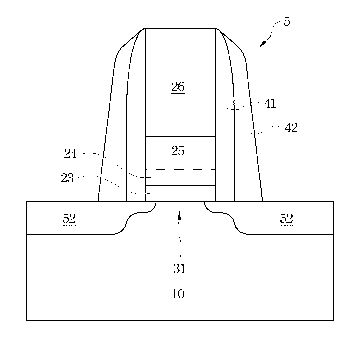
[0017]The present invention will be described with respect to various embodiments in a specific context, namely, germanium channel field effect transistors. The invention may also be applied, however, to other types of devices and channel materials.

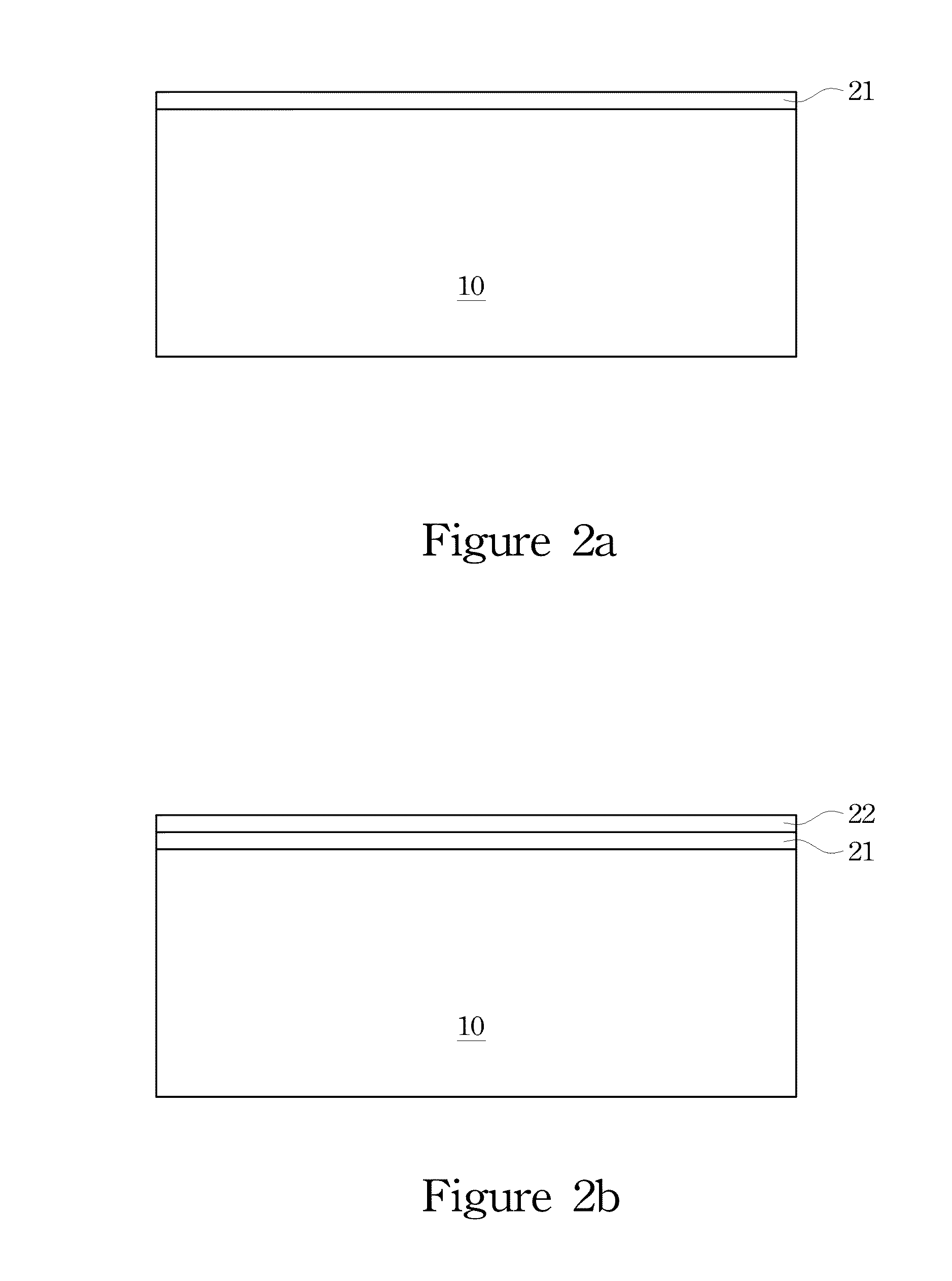
[0018]One of the challenges in forming germanium transistors is to form gate dielectrics with a high dielectric constant without introducing defects such as interface states or bulk charge traps. However, unlike silicon, germanium does not form stable oxides with low defect density. Rather, germanium dioxide has a high defect densi...


PUM

PropertyMeasurementUnit
temperaturesaaaaaaaaaa
dielectric constantaaaaaaaaaa

Abstract

Germanium field effect transistors and methods of fabricating them are described. In one embodiment, the method includes forming a germanium oxide layer over a substrate and forming a metal oxide layer over the germanium oxide layer. The germanium oxide layer and the metal oxide layer are converted into a first dielectric layer. A first electrode layer is deposited over the first dielectric layer.

Description

[0001]This application claims the benefit of U.S. Provisional Application No. 61 / 161,253, entitled “Germanium Field Effect Transistors and Fabrication Thereof,” filed on Mar. 18, 2009, which is incorporated herein by reference.TECHNICAL FIELD[0002]The present invention relates generally to semiconductor devices, and more particularly to germanium field effect transistors, and methods of fabrication thereof.BACKGROUND[0003]The semiconductor industry is facing unprecedented challenges due to the limitations of traditional transistor scaling arising from non-scaling of conventional materials (e.g., gate oxide). The industry has aggressively adopted new methods for performance enhancements, like strained silicon. However, continued scaling with strain is expected to be challenging due to increase in defectivity and possible saturation of strain effects. Hence, there is a renewed interest in the integration of group III-V semiconductors and / or group IV semiconductors as new channel mater...

Claims


Application Information

Patent Timeline
Patent Type & Authority Applications(United States)
IPC IPC(8): H01L29/78H01L21/28
CPCH01L21/02175H01L29/16H01L29/4966H01L21/28255H01L29/517H01L29/6659H01L29/7833H01L29/513
Inventor LIN, JING-CHENG
Owner TAIWAN SEMICON MFG CO LTD
Why Eureka
Try Eureka