Light emitting diode package structure and manufacturing method thereof

a technology of light-emitting diodes and package structures, applied in the direction of discharge tubes/lamp details, discharge tubes luminescnet screens, coatings, etc., can solve the problem of uniform distribution of fluorescent materials, and achieve the effect of enhancing the light-emitting uniformity of led package structures

Inactive Publication Date: 2010-09-23
EVERLIGHT ELECTRONICS
View PDF14 Cites 37 Cited by
  • Summary
  • Abstract
  • Description
  • Claims
  • Application Information

AI Technical Summary

Benefits of technology

[0008]The present invention provides a LED package structure and a method of fabricating the same, so as to enhance the light-emitting uniformity of the LED package structure.
[0031]In view of above, in the present invention, the phosphor solution is sprayed on the light emitting surface and the side surfaces of the LED chip, and the fluorescent layer has substantially the same thickness on the light emitting surface and the side surfaces of the LED chip. That is, the fluorescent layer is disposed on the emitting surface and the side surfaces of the LED chip with a uniform thickness, and the thickness of the fluorescent layer on the light emitting layer is substantially the same as that on each side surface. Therefore, when the light emitted from the LED chip is transmitted to the external environment through the molding compound, the LED package structure has better light emitting uniformity.

Problems solved by technology

Accordingly, the distribution of the fluorescent material is not uniform.

Method used


Image

  • Light emitting diode package structure and manufacturing method thereof
  • Light emitting diode package structure and manufacturing method thereof
  • Light emitting diode package structure and manufacturing method thereof

Examples


Embodiment Construction

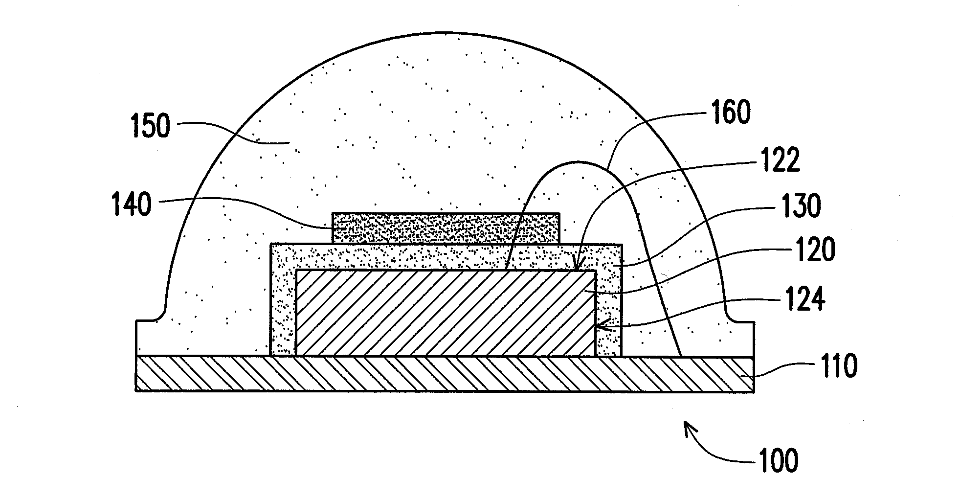
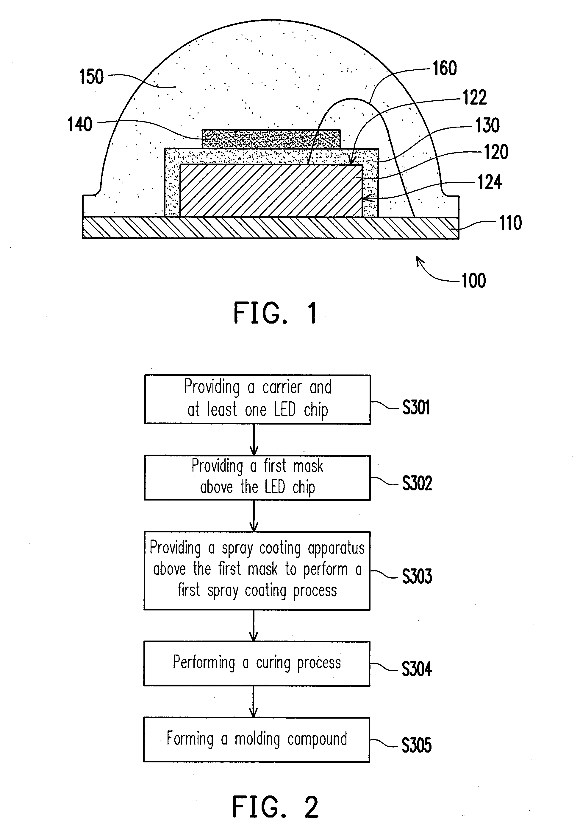
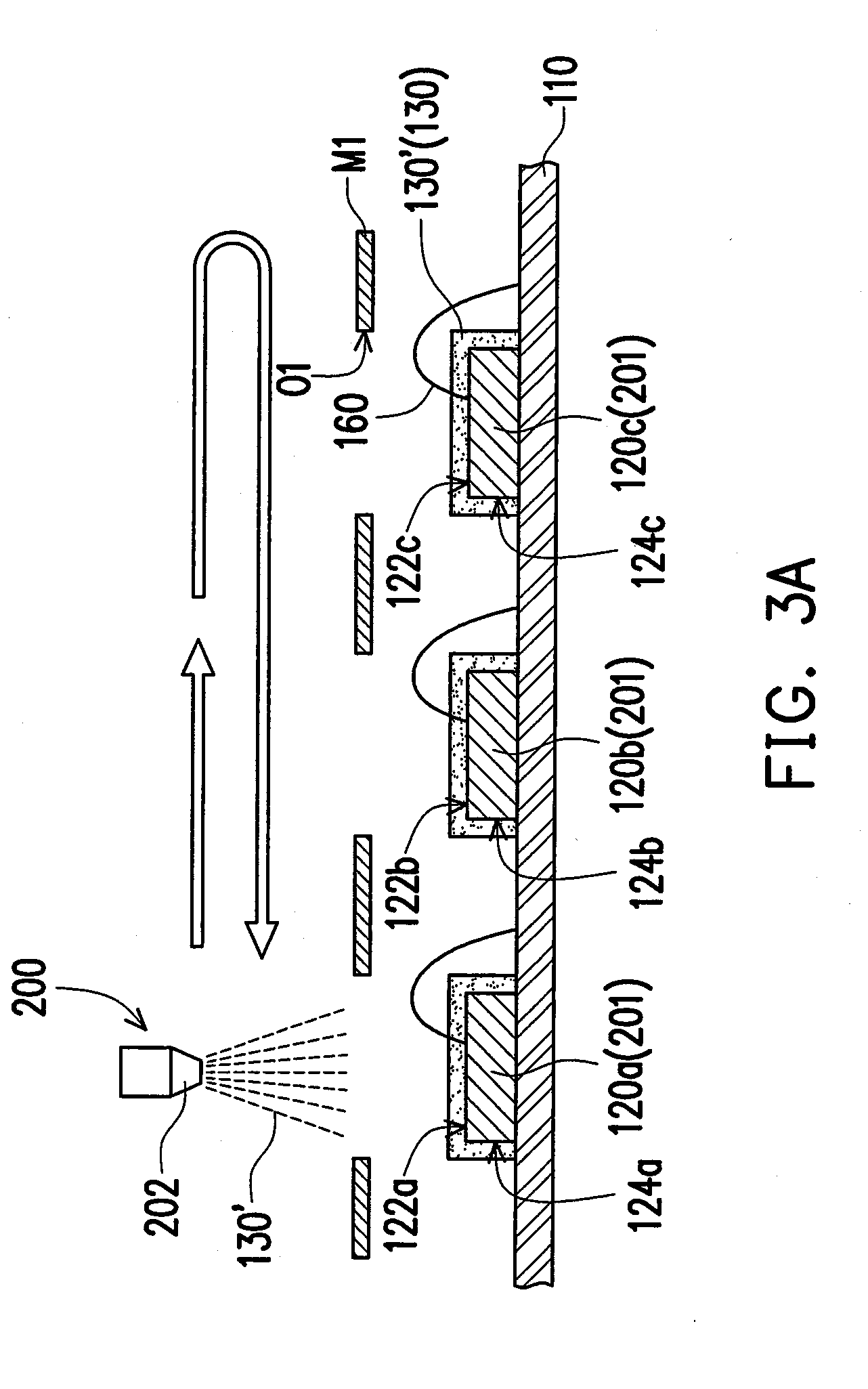
[0037]FIG. 1 schematically illustrates a cross-sectional view of a LED package structure according to an embodiment of the present invention. Referring to FIG. 1, the LED package structure 100 includes a carrier 110, a LED chip 120, a first fluorescent layer 130, a second fluorescent layer 140 and a lens, for example a molding compound 150.

[0038]In details, the LED chip 120 is disposed on the carrier 110. The LED chip 120 has a light emitting surface 122 and a plurality of side surfaces 124 connected to the light emitting surface 122. The LED chip 120 is electrically connected to the carrier 110 through at least one wire 160 (FIG. 1 only schematically illustrates one wire for illustration purposes). In this embodiment, the carrier 110 is a circuit board or a lead frame, for example. The LED chip 120 includes a blue LED chip, a red LED chip, a green LED chip or a purple LED chip, for example.

[0039]The first fluorescent layer 130 is disposed on the LED chip 120 and conformally covers ...


PUM


Abstract

A method of fabricating a light emitting diode (LED) package structure is provided. A carrier and at least one LED chip having a light emitting surface and a plurality of side surfaces are provided. A first mask having at least one first opening is provided, and the first opening at least exposes the LED chip. A spray coating apparatus is provided above the first mask to perform a first spray coating process. The spray coating apparatus moves back and forth to spray a first phosphor solution over the LED chip so that the light-emitting surface and the side surfaces of the LED chip can be conformally covered by the sprayed first phosphor solution. The first phosphor solution is cured to form a first fluorescent layer by performing a curing process. A molding compound is formed to encapsulate the first fluorescent layer and a portion of the carrier.

Description

CROSS-REFERENCE TO RELATED APPLICATION[0001]This application claims the priority benefit of Taiwan application serial no. 98109175, filed on Mar. 20, 2009. The entirety of the above-mentioned patent application is hereby incorporated by reference herein and made a part of specification.BACKGROUND OF THE INVENTION[0002]1. Field of Invention[0003]The present invention relates to a semiconductor package structure and a manufacturing method thereof, and more generally to a light emitting diode (LED) package structure and a manufacturing method thereof.[0004]2. Description of Related Art[0005]Since a light emitting diode (LED) has such advantages as long service life, small volume, high shock resistance, low heat output and low power consumption, it has been widely applied in indicators or light sources for household appliances and various equipment. In recent years, the LED has been developed towards multicolor and high brightness; therefore, its application scope has been expanded to l...

Claims


Application Information

Patent Timeline
Patent Type & Authority Applications(United States)
IPC IPC(8): H01J1/62B05D5/06
CPCH01L33/504H01L33/52H01L2933/0041H01L2224/48091H01L2224/8592H01L2924/00014H01L2924/181H01L2924/00012
Inventor CHAO, TZU-HAO
Owner EVERLIGHT ELECTRONICS
Why Eureka
Try Eureka