Duty detection circuit, clock generation circuit including the duty detection circuit, and semiconductor device

Active Publication Date: 2010-09-23
LONGITUDE SEMICON S A R L
View PDF15 Cites 18 Cited by
  • Summary
  • Abstract
  • Description
  • Claims
  • Application Information

AI Technical Summary

Benefits of technology

[0015]According to the present invention, the plurality of duty detectors operate in different phases. Therefore, the output selecting unit can output a duty detection signal with a higher frequency than a frequency with which each duty detector generates the duty detection signal. Accordingly, when the duty detection circuit according to the present invention is used to adjust clocks of the DLL circuit, a control period of the DLL circuit ca

Problems solved by technology

Furthermore, when nine cycles are necessary to adjust the rising edge of the internal clock, then a correct duty detection signal cannot be obtained promptly in the ninth cycle, and it is the 12th cycle when the duty detection signal is updated next to the eighth cycle.
Moreover, when jitter is to be suppressed

Method used


Image

  • Duty detection circuit, clock generation circuit including the duty detection circuit, and semiconductor device
  • Duty detection circuit, clock generation circuit including the duty detection circuit, and semiconductor device
  • Duty detection circuit, clock generation circuit including the duty detection circuit, and semiconductor device

Examples


Example

[0030]Preferred embodiments of the present invention will be explained below in detail with reference to the accompanying drawings.

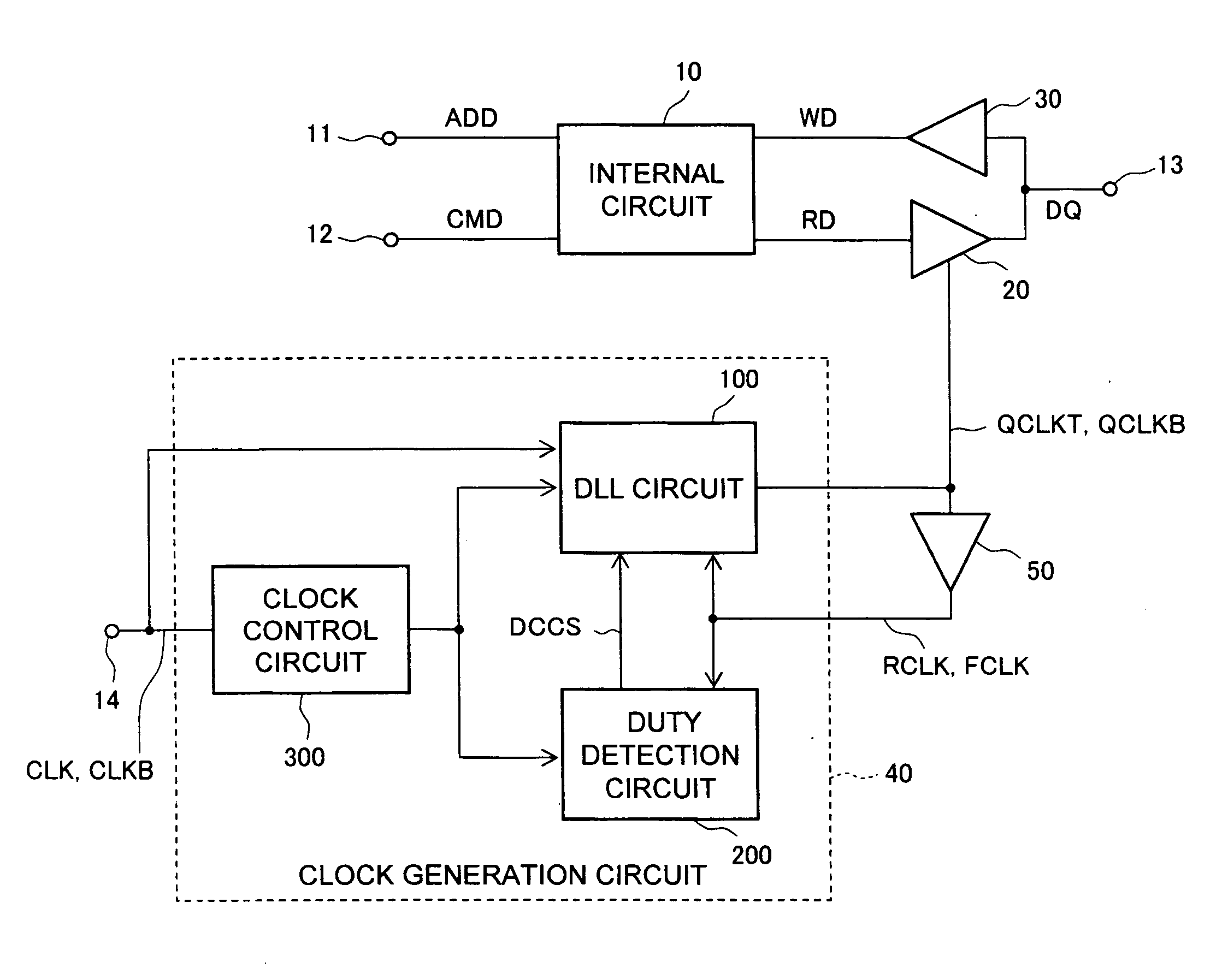
[0031]FIG. 1 is a block diagram showing a configuration of a semiconductor device according to an embodiment of the present invention.

[0032]The semiconductor device according to the present invention is a DDR synchronous memory device although not limited thereto. The semiconductor device includes an internal circuit 10, an output buffer 20, an input buffer 30, a clock generation circuit 40, and a replica buffer 50.

[0033]The internal circuit 10 is a circuit block for realizing main functions of the semiconductor device. In the present embodiment, the internal circuit 10 includes a memory cell array, an address decoder, a command decoder, a data amplifier and the like. Therefore, the internal circuit 10 according to the present embodiment operates based on an address signal ADD and a command signal CMD supplied from an address terminal 11 and a command te...


PUM


Abstract

To provide a duty detection circuit including: a plurality of duty detectors that detect a duty ratio of internal clocks; a controller that controls the plurality of duty detectors so that the plurality of duty detectors operates in different phases from one another; and an output selecting unit that selects one of duty detection signals from the plurality of duty detectors. According to the present invention, since the duty detectors operate in the different phases from one another, the output selecting unit can output a duty detection signal with a higher frequency than a generation frequency with which each duty detector generates the duty detection signal. Accordingly, when the duty detection circuit according to the present invention is used to adjust a clock of the DLL circuit, a control period of the DLL circuit can be reduced.

Description

BACKGROUND OF THE INVENTION[0001]1. Field of the Invention[0002]The present invention relates to a duty detection circuit capable of generating a duty detection signal with high frequency, and a clock generation circuit including the same. The present invention also relates to a semiconductor device including the clock generation circuit.[0003]2. Description of Related Art[0004]In recent years, a synchronous memory that operates synchronously with a clock has been widely used as a main memory of personal computers or the like. Particularly in a DDR (Double Date Rate) synchronous memory, it is necessary to accurately synchronize input / output data with an external clock. Therefore, a DLL (Delay Locked Loop) circuit that generates an internal clock synchronous with the external clock is employed.[0005]A DLL circuit of a certain type adjusts a rising edge of an internal clock based on a result of phase comparison, and adjusts a falling edge of the internal clock based on a result of dut...

Claims


Application Information

Patent Timeline
IPC IPC(8): H03L7/06H03K3/017
CPCH03K3/017H03K17/005H03L7/0818H03L7/087H03L7/10H03L7/0814
Inventor MONMA, ATSUKO
Owner LONGITUDE SEMICON S A R L
Why Eureka
Try Eureka