
Eureka
For R&D, Eureka makes reading and utilizing patents & technical documents easy.
Eureka AIR
Designed for self-driven R&D workflows. Generate viable solutions, solve complex R&D challenges, empower your innovation with AI.

Eureka Materials
Designed for material experts only. Revolutionize your material R&D, from search, analyze, to developing new materials.

TechResearch
Generate reliable direction feasibility study reports for your R&D in just a few steps.

TechSeek
Discover and master advanced knowledge NOW. Basics, ideas, possibilities, all at once.

TechMind
As an expert in R&D Theories, TechMind can generates customized viable solutions instantly.

TechRisk
Analyze your overall solution with one click, know your potential R&D risks in advance.

TechMonitor
Get weekly tech updates, stay abreast of the latest tech innovations and key insights.
Composite alloy bonding wire and manufacturing method thereof
- Summary
- Abstract
- Description
- Claims
- Application Information
AI Technical Summary
Benefits of technology
Problems solved by technology
Method used
Image

Examples
embodiment 1
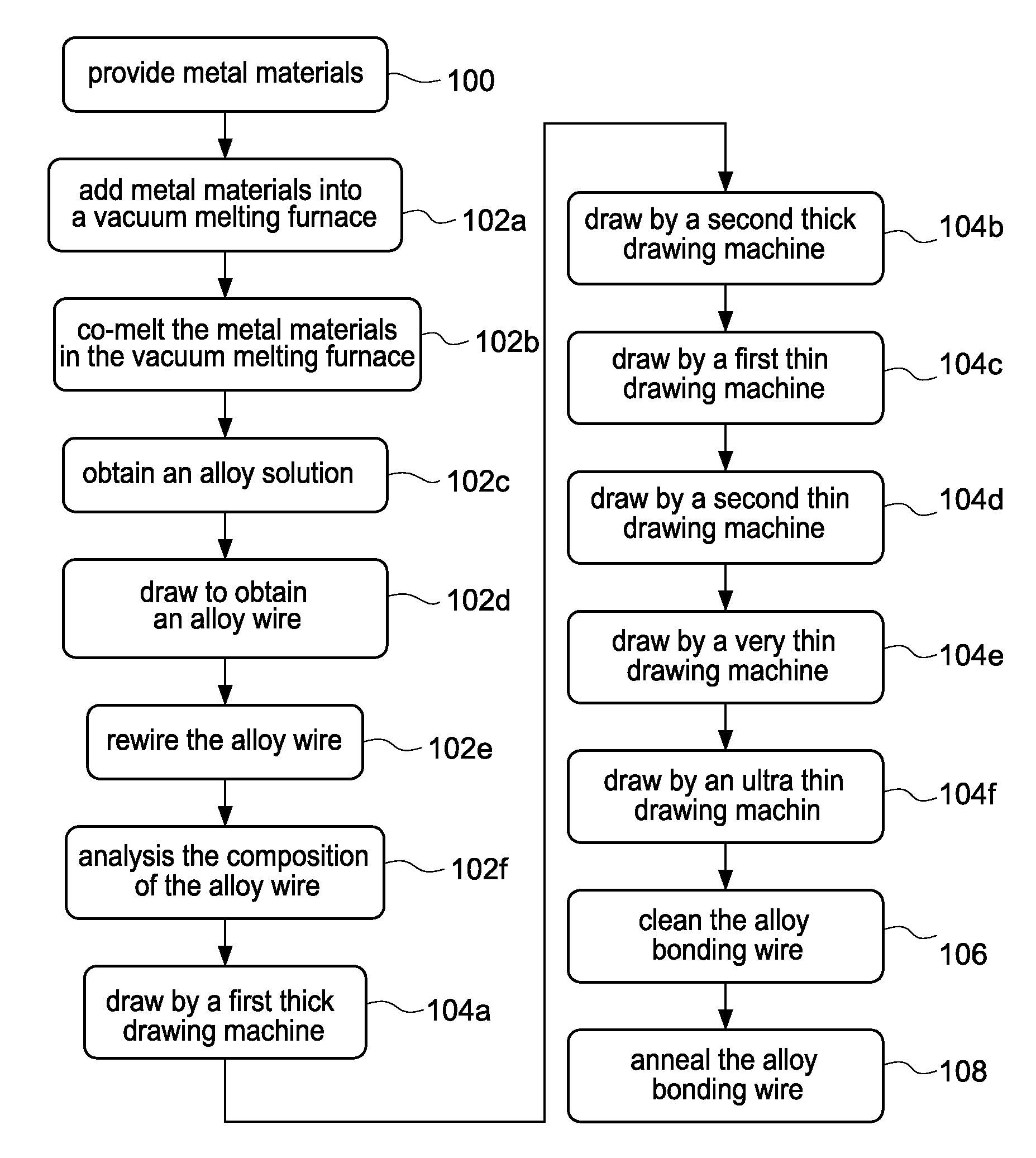
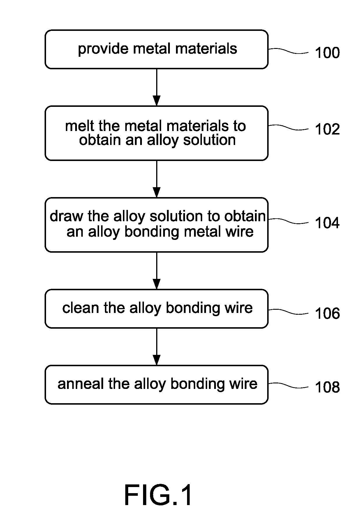
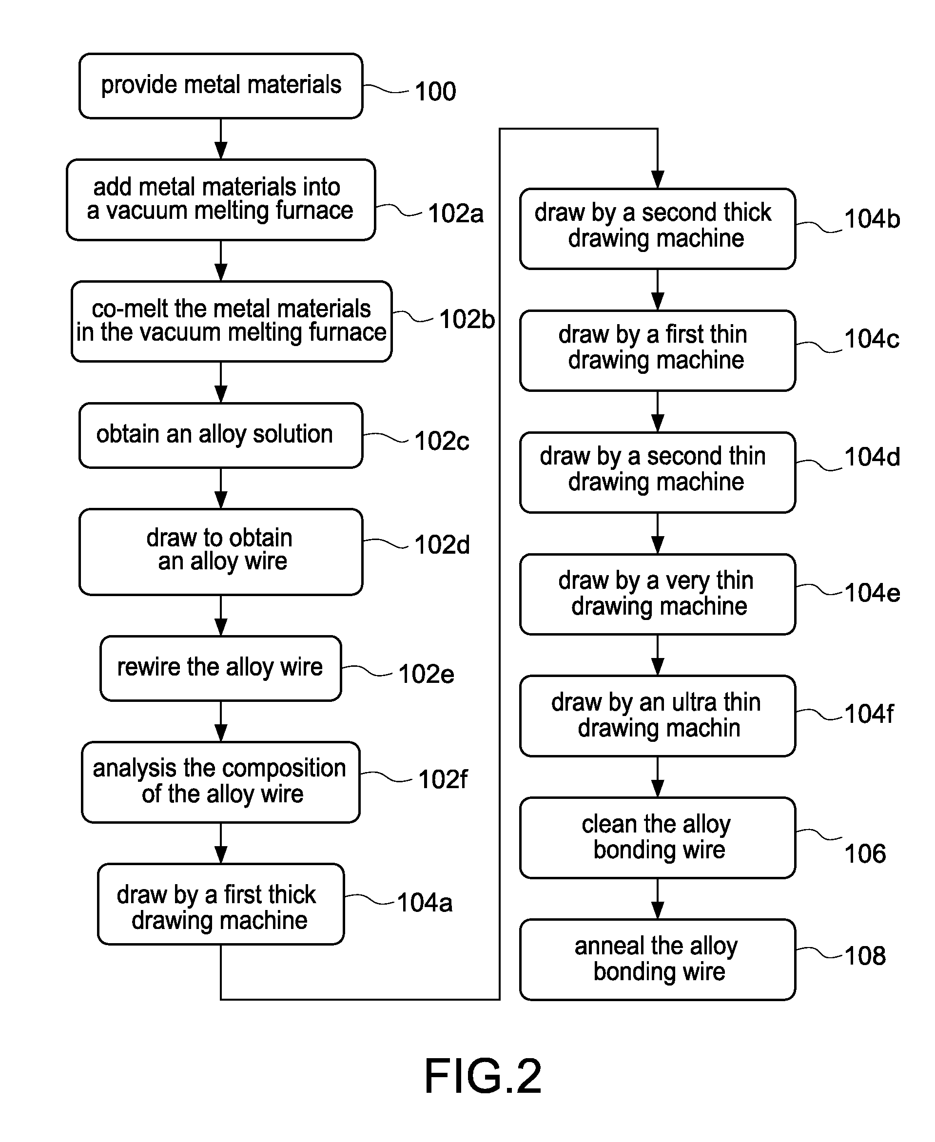
[0024]A primary material of Ag is provided and is melted in a vacuum melting furnace. Then, specific amount of a secondary metal material of Pd is added into the vacuum melting furnace, and is co-melted with the primary material in the vacuum melting furnace to obtain a Ag—Pd alloy solution. The Ag—Pd alloy solution consists of: 99.99 wt. % Ag and 0.001 wt. % Pd.
[0025]Continuous casting and drawing processes are performed on the Ag—Pd alloy solution to obtain a Ag—Pd alloy wire with a diameter of 4 mm. The Ag—Pd alloy wire is rewired by a reeling machine and then composition analysis is performed on the Ag—Pd alloy wire to check if the obtained composition meets the requirement.
[0026]A drawing process is performed on the Ag—Pd alloy wire; the obtained Ag—Pd alloy wire with a diameter of 4 mm is drawn by a first thick drawing machine to obtain a Ag—Pd alloy wire with a diameter of 3 mm. The Ag—Pd alloy wire with a diameter of 3 mm is drawn by a second thick drawing machine to obtain ...
embodiment 2
[0028]A primary material of Ag is provided and is melted in a vacuum melting furnace. Then, specific amount of a secondary metal material of Pd is added into the vacuum melting furnace, and is co-melted with the primary material in the vacuum melting furnace to obtain a Ag—Pd alloy solution. The Ag—Pd alloy solution consists of: 95.00 wt. % Ag and 5.00 wt. % Pd.
[0029]Continuous casting and drawing processes are performed on the Ag—Pd alloy solution to obtain a Ag—Pd alloy wire with a diameter of 6 mm. The Ag—Pd alloy wire is rewired by a reeling machine and then composition analysis is performed on the Ag—Pd alloy wire to check if the obtained composition meets the requirement.
[0030]A drawing process is performed on the Ag—Pd alloy wire; the obtained Ag—Pd alloy wire with a diameter of 6 mm is drawn by a first thick drawing machine to obtain a Ag—Pd alloy wire with a diameter of 3 mm. The Ag—Pd alloy wire with a diameter of 3 mm is drawn by a second thick drawing machine to obtain a...
embodiment 3
[0032]A primary material of Ag is provided and is melted in a vacuum melting furnace. Then, specific amount of a secondary metal material of Pd is added into the vacuum melting furnace, and is co-melted with the primary material in the vacuum melting furnace to obtain a Ag—Pd alloy solution. The Ag—Pd alloy solution consists of: 90.00 wt. % Ag and 10.00 wt. % Pd.
[0033]Continuous casting and drawing processes are performed on the Ag—Pd solution to obtain a Ag—Pd alloy wire with a diameter of 8 mm. The Ag—Pd alloy wire is rewired by a reeling machine and then composition analysis is performed on the Ag—Pd alloy wire to check if the obtained composition meets the requirement.
[0034]A drawing process is performed on the Ag—Pd alloy wire; the obtained Ag—Pd alloy wire with a diameter of 8 mm is drawn by a first thick drawing machine to obtain a Ag—Pd alloy wire with a diameter of 2 mm. The Ag—Pd alloy wire with a diameter of 2 mm is drawn by a second thick drawing machine to obtain a Ag—P...
PUM
| Property | Measurement | Unit |
|---|---|---|
| Length | aaaaa | aaaaa |
| Length | aaaaa | aaaaa |
| Length | aaaaa | aaaaa |
Abstract
Description
Claims
Application Information
 - R&D Engineer
- R&D Manager
- IP Professional
- Industry Leading Data Capabilities
- Powerful AI technology
- Patent DNA Extraction
Browse by: Latest US Patents, China's latest patents, Technical Efficacy Thesaurus, Application Domain, Technology Topic, Popular Technical Reports.
© 2024 PatSnap. All rights reserved.Legal|Privacy policy|Modern Slavery Act Transparency Statement|Sitemap|About US| Contact US: help@patsnap.com