Eureka AIR delivers breakthrough ideas for toughest innovation challenges, trusted by R&D personnel around the world.

Power Storage Device and Manufacturing Method Thereof

a technology of power storage device and manufacturing method, which is applied in the manufacture of secondary cells, climate sustainability, final product manufacturing, etc., can solve the problem that the power storage device formed over such substrates is also thick, and achieve the effect of small thickness and small thickness

Active Publication Date: 2010-09-23
SEMICON ENERGY LAB CO LTD
View PDF31 Cites 67 Cited by
  • Summary
  • Abstract
  • Description
  • Claims
  • Application Information

AI Technical Summary

Benefits of technology

[0014]It is also an object of one embodiment of the present invention disclosed in this specification to reduce the size, thickness, and weight of an electric device which incorporates the power storage device.
[0018]According to one embodiment of the present invention disclosed in this specification, a power storage device having a small thickness can be manufactured. Further, by incorporating such a power storage device having a small thickness, a miniaturized electric device can be manufactured.

Problems solved by technology

Such substrates are thick, and thus the power storage devices formed over such substrates are also thick.

Method used


Image

  • Power Storage Device and Manufacturing Method Thereof
  • Power Storage Device and Manufacturing Method Thereof
  • Power Storage Device and Manufacturing Method Thereof

Examples


embodiment 1

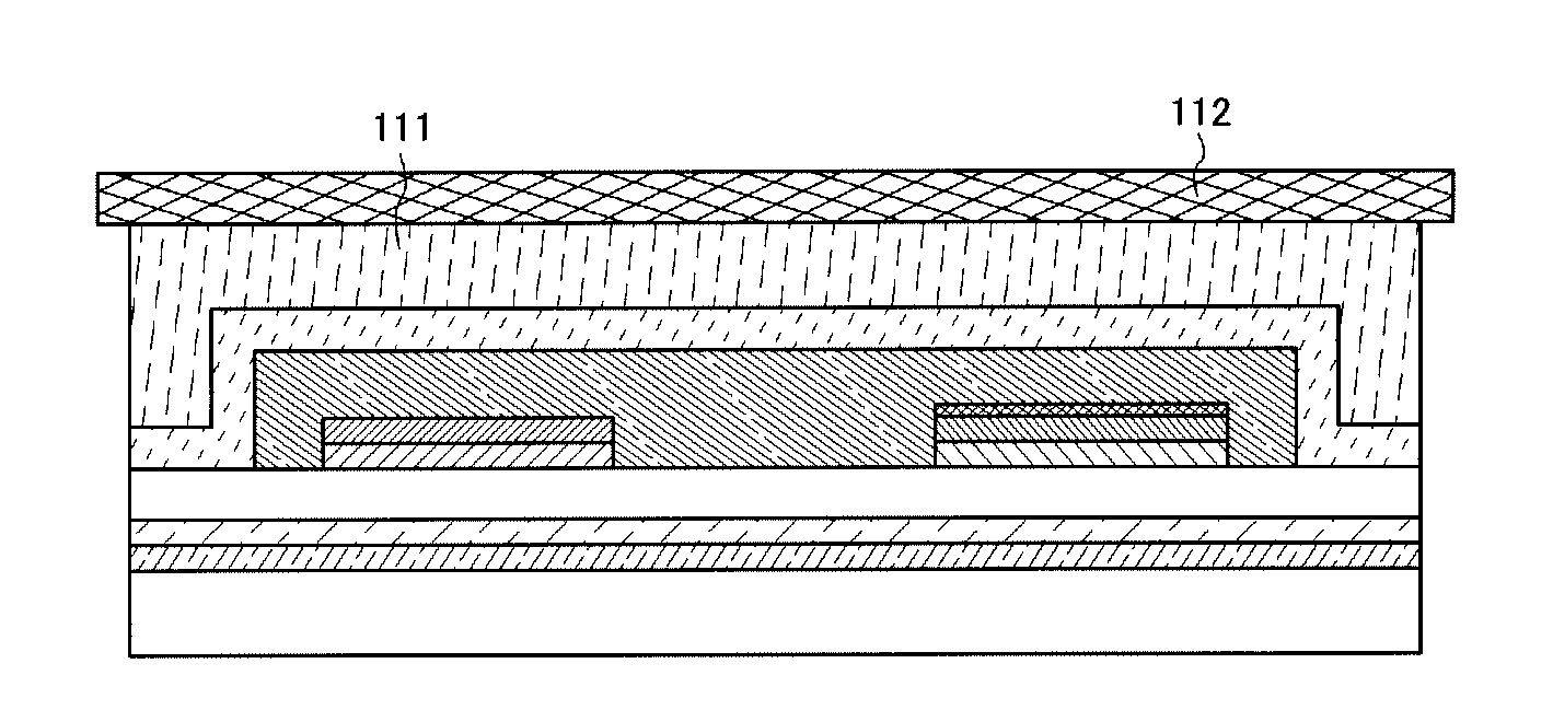
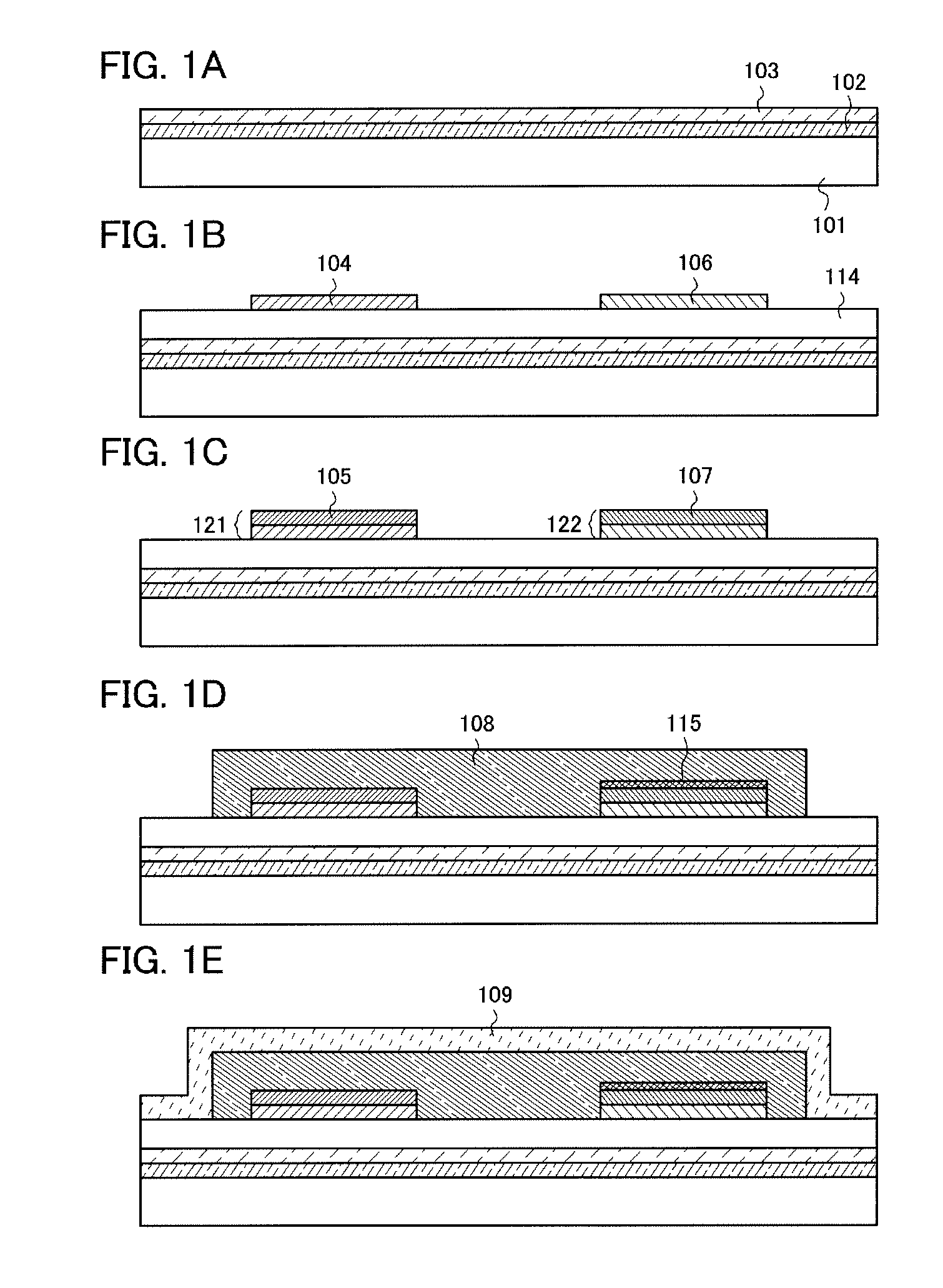
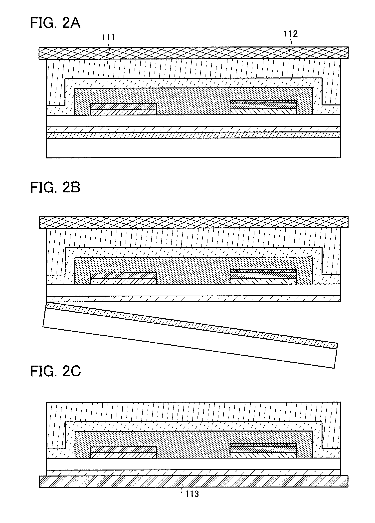
[0024]This embodiment will be described with reference to FIGS. 1A to 1E, FIGS. 2A to 2C, and FIG. 3.

[0025]First, a first layer 102 and a second layer 103 which have low adhesiveness to each other are formed over a substrate 101 (FIG. 1A).

[0026]The substrate 101 can be a glass substrate, a quartz substrate, a plastic substrate, or the like having an insulating surface. Additionally, a conductive substrate of metal or the like or a substrate in which an insulating film is formed over a semiconductor substrate of silicon or the like can be used.

[0027]At the interface between the first layer 102 and the second layer 103 which have low adhesiveness to each other, the first layer 102 and the second layer 103 can be separated from each other, so that the substrate 101 and the first layer 102 can be separated from a stacked structure formed over the second layer 103.

[0028]Examples of the combination of the first layer 102 and the second layer 103 which have low adhesiveness to each other i...


PUM

PropertyMeasurementUnit
thickaaaaaaaaaa
thicknessaaaaaaaaaa
flexibleaaaaaaaaaa

Abstract

A power storage device having a small thickness is manufactured. A manufacturing method of the power storage device includes: forming a first layer and a second layer over a first substrate; forming a first insulating layer, a positive electrode and a negative electrode over the second layer; forming a solid electrolyte layer over the first insulating layer, the positive electrode, and the negative electrode; forming a sealing layer to cover the solid electrolyte layer; forming a planarization film and a support over the sealing layer; separating the first layer and the second layer from each other so that the second layer, the positive electrode, the negative electrode, the solid electrolyte layer, the sealing layer, the planarization film, and the support are separated from the first substrate; attaching the separated structure to a second substrate which is flexible; and separating the support from the planarization film.

Description

BACKGROUND OF THE INVENTION[0001]1. Field of the Invention[0002]The present invention disclosed in this specification relates to power storage devices.[0003]2. Description of the Related Art[0004]In recent years, power storage devices such as lithium-ion secondary batteries where carbon or lithium metal oxide is used as a battery material and which are charged and discharged by the movement of lithium ions as carrier ions between a positive electrode and a negative electrode, and electrochemical capacitors, have been actively developed (see Patent Documents 1 to 3).[0005]Further, among such lithium-ion secondary batteries, all-solid-state lithium-ion secondary batteries in which a solid electrolyte is used instead of a liquid electrolyte have been developed (see Patent Documents 4 to 6 and Non-Patent Document 1).REFERENCESPatent Documents[0006][Patent Document 1] Japanese Published Patent Application No. 2008-294314[0007][Patent Document 2] Japanese Published Patent Application No. ...

Claims


Application Information

Patent Timeline
Patent Type & Authority Applications(United States)
IPC IPC(8): H01M4/02H01M2/00H01G11/00H01G11/06H01G11/56H01G11/78H01G11/84H01M2/02H01M10/0562H01M10/0565H01M10/0585
CPCH01G9/016H01G9/155H01G11/28H01G11/56H01G11/68Y10T29/49115H01G11/84H01M4/661H01M10/0436H01M10/0525Y02E60/13H01G11/80Y02E60/10Y02P70/50H01G11/74C23C14/0676C23C14/10C23C14/14C23C14/34C23C14/58H01G11/86H01M10/0562H01M10/0585
Inventor IZUMI, KONAMI
Owner SEMICON ENERGY LAB CO LTD
Why Eureka
Eureka Blog
Learn More