Semiconductor device and manufacturing method thereof

a semiconductor and manufacturing method technology, applied in the direction of semiconductor devices, semiconductor/solid-state device details, diodes, etc., can solve the problems of reducing difficult to evenly disperse soft magnetic powder, and deterioration of the effect of eddy-current loss at a portion where soft magnetic powder is scarcely dispersed, etc., to prevent short circuit, reduce the eddy current generation of thin film inductors in semiconductor substrates

Inactive Publication Date: 2010-09-30
TERAMIKROS INC
View PDF3 Cites 10 Cited by
  • Summary
  • Abstract
  • Description
  • Claims
  • Application Information

AI Technical Summary

Benefits of technology

[0019]According to the aspects of the present invention, the thin film inductor is provided on the second resin film which is provided over the upper surface of the first resin film except at least the peripheral portion thereof, on the semiconductor substrate. Thus, the eddy-current loss of the thin film inductor due to the eddy current generated in the semiconductor...

Problems solved by technology

However, in the above described semiconductor device, the magnetic film is manufactured by mixing the soft magnetic power which is a relatively expensive material into the thermosetting resin made of polyimide system resin, and the like, thereby the semiconductor device results i...

Method used


Image

  • Semiconductor device and manufacturing method thereof
  • Semiconductor device and manufacturing method thereof
  • Semiconductor device and manufacturing method thereof

Examples


first embodiment

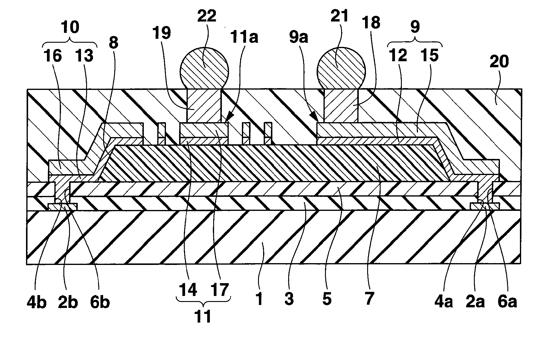
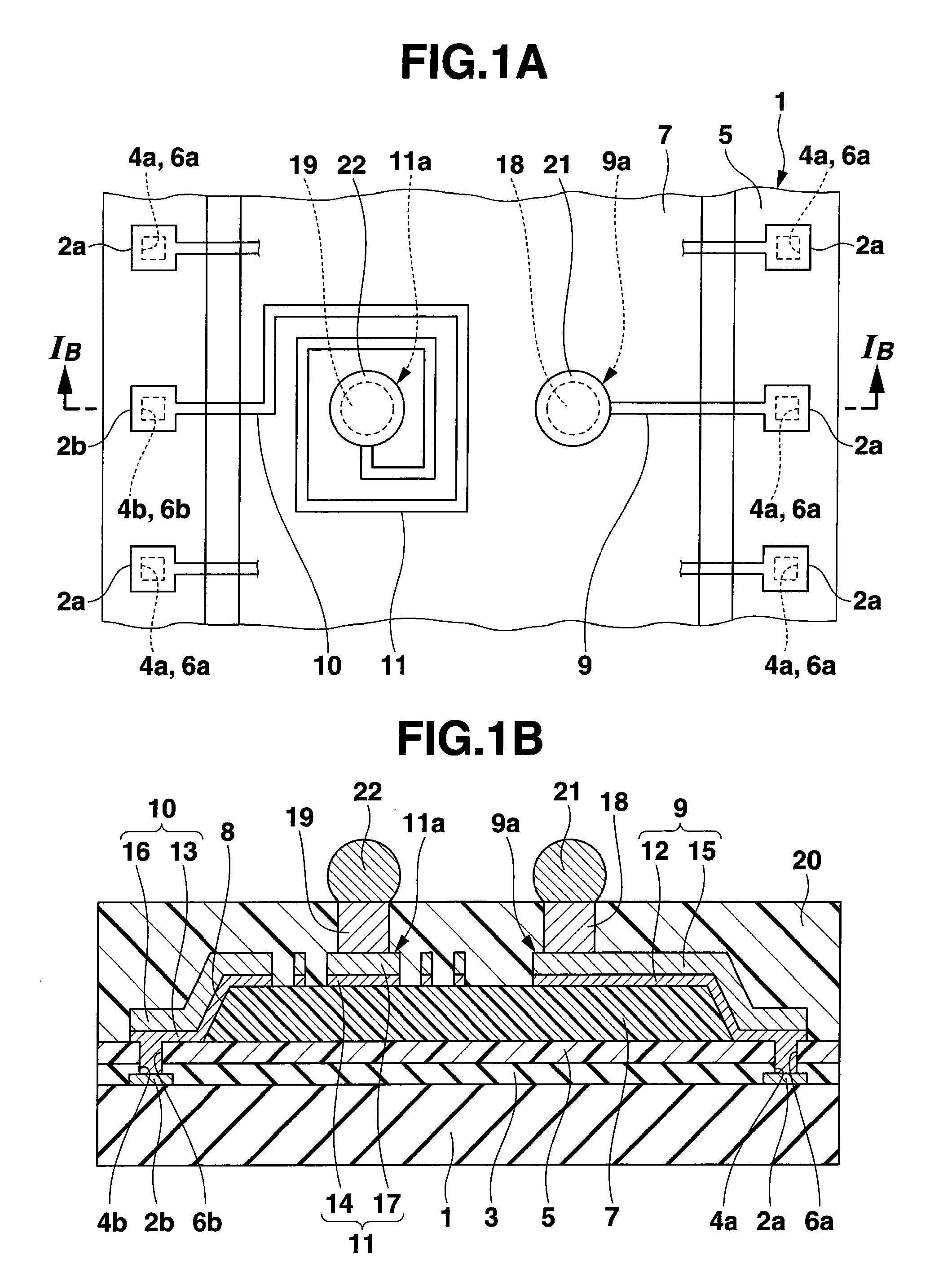
[0041]FIG. 1A is a plan view of a main part of a semiconductor device according to a first embodiment of the present invention (which is in a state where a sealing film is removed from the semiconductor device shown in FIG. 1B).

[0042]FIG. 1B is a sectional diagram along B-B line of FIG. 1A.

[0043]This semiconductor device is what is generally called a chip size package (CSP), and comprises a silicon substrate (semiconductor substrate) 1 having a plane rectangular form. An element which comprises an integrated circuit having predetermined functions such as a circuit element, for example, a transistor, a diode, a resistor, a capacitor, and the like, is provided in an upper surface of the silicon substrate 1. Further, a plurality of connection pads 2a, 2b formed of aluminum system metal, and the like, are provided in the periphery portion of the upper surface so as to be connected to the integrated circuit. In this case, the connection pad shown as the reference character 2b is connecte...

second embodiment

[0070]FIG. 13A is a plan view of a main part of a semiconductor device according to a second embodiment of the present invention (which is in a state where a sealing film is removed from the semiconductor device shown in FIG. 13B).

[0071]FIG. 13B is a sectional diagram along B-B line of FIG. 13A.

[0072]The remarkable difference of this semiconductor device from the semiconductor device shown in FIGS. 1A, 1B is that not only the external edge portion but also the internal edge portion of the thin film inductor 11 having the spiral form is connected to the connection pads which is connected to the integrated circuit formed on the upper surface of the silicon substrate 1.

[0073]That is to say, the connection pads indicated by the reference characters 2b, 2c are connected to the internal edge portion and the external edge portion of the thin film inductor 11 having the spiral form. In FIG. 13A, the connection pads 2b, 2c are disposed in a state of being adjacent to each other. The passivat...


PUM


Abstract

Disclosed is a semiconductor device comprising: a semiconductor substrate in which an integrated circuit is formed; a first resin film provided over the semiconductor substrate; a second resin film provided over an upper surface of the first resin film except at least a peripheral portion of the first resin film; and a thin film inductor provided over the second resin film.

Description

CROSS-REFERENCE TO RELATED APPLICATIONS[0001]This application is based upon and claims the benefit of priority under 35 USC 119 of Japanese Patent Application No. 2009-075277 filed on Mar. 25, 2009, the entire disclosure of which, including the description, claims, drawings, and abstract, is incorporated herein by reference in its entirety.BACKGROUND OF THE INVENTION[0002]1. Field of the Invention[0003]The present invention relates to a semiconductor device and a manufacturing method of the semiconductor device.[0004]2. Description of the Related Art[0005]Conventionally, a semiconductor device which is equipped with a thin film inductor having a spiral form, referred to as a chip size package (CSP), has been known. Such semiconductor device is disclosed, for example, in Japanese Patent Application Laid-open Publication No. 2008-210828. This semiconductor device comprises a semiconductor substrate. An insulation film is provided on an upper surface of the semiconductor substrate. A p...

Claims


Application Information

Patent Timeline
IPC IPC(8): H01L29/86H01L21/02
CPCH01L23/3114H01L2224/0236H01L24/11H01L24/13H01L24/94H01L2224/94H01L2924/01002H01L2924/01013H01L2924/01029H01L2924/01078H01L2924/14H01L2924/19041H01L23/5227H01L2224/024H01L2224/11H01L2224/03
Inventor MIHARA, ICHIRO
Owner TERAMIKROS INC
Why Eureka
Try Eureka