Stacked multichip package

a multi-chip, stacking technology, applied in the direction of semiconductor devices, semiconductor/solid-state device details, electrical apparatus, etc., can solve the problems of increasing manufacturing cost and risk lowering manufacturing yield, increasing manufacturing cost and risk, and increasing the risk of low manufacturing yield. , to achieve the effect of high yield and high yield

Inactive Publication Date: 2010-09-30
CHIPMOS TECH INC
View PDF4 Cites 84 Cited by
  • Summary
  • Abstract
  • Description
  • Claims
  • Application Information

AI Technical Summary

Benefits of technology

[0009]The present invention provides a stacked multichip package, which uses a chip carrier to carrier a chip stacked above another chip disposed on a substrate to form a stacked multichip package. The stacked multichip package of the present invention built using high yield chip package technique and chip stack technique has an advantage of high yield.

Problems solved by technology

Such additional processes increase manufacturing cost and risk lowering manufacturing yield.
When multiple chips are packaged into an encapsulation body, the result of composite manufacturing yields greatly influences manufacturing cost.
In particular, when the encapsulation body includes a high-priced chip, the risk of low manufacturing yield is more important.
If a low price chip in the encapsulation body malfunctions or if a chip is damaged during the chip stacking process, the high-priced chip will have to be discarded with the nonfunctional chip, and such discard causes serious impact to the manufacturing cost.

Method used


Image

  • Stacked multichip package
  • Stacked multichip package

Examples


Embodiment Construction

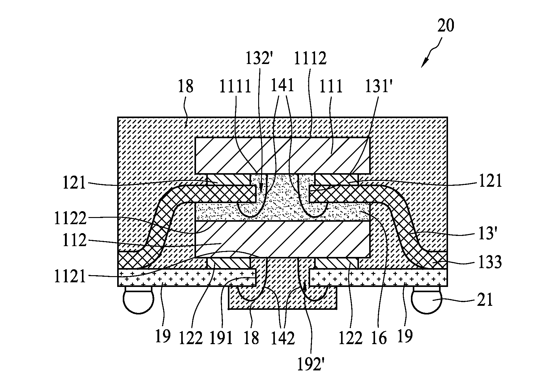
[0019]FIG. 1 is a cross sectional view showing a stacked multichip package 10 according to the first embodiment of the present invention. The stacked multichip package 10 of the first embodiment of the present invention comprises a first chip 111, a first chip carrier 13, a plurality of first conductive leads 141, a second chip 112, an adhesive layer 16, a second chip carrier 19, and a plurality of second conductive leads 142. The first chip 111 comprises a first active surface 1111 and a first rear surface 1112 opposite to the first active surface 1111. An integrated circuit including a plurality of electronic components and conductive traces connecting the electronic components is formed on the first active surface 1111. The first chip carrier 13 includes an inner wall 131 defining a first opening 132. The first active surface 1111 of the first chip 111 faces toward the first opening 132, and is attached to the first chip carrier 13. In the present embodiment, the first chip 111 a...


PUM


Abstract

A stacked multichip package comprises a first chip having a first active surface and a first rear surface, a first chip carrier having a first opening and being configured to carrier the first active surface, a plurality of first conductive leads passing through the first opening and being configured to electrically connect the first active surface and the first chip carrier, a second chip having a second active surface and a second rear surface, an adhesive layer configured to enclose the first conductive leads and to electrically couple the first chip carrier to the second rear surface, a second chip carrier having a second opening and being electrically connected to the second active surface, and a plurality of conductive leads passing through the second opening and being configured to electrically connect the second active surface and the second chip carrier.

Description

BACKGROUND OF THE INVENTION[0001]1. Field of the Invention[0002]The present invention relates to a semiconductor chip package, and relates more particularly to a stacked multichip package.[0003]2. Description of the Related Art[0004]Integration of multiple stacked chips into a single package can increase electronic component package density and reduce the signal distances between electronic components. In other words, the integration technique can not only decrease the total volume required to prepare for individual chips, but can also improve the integral performance of the chips. Among the techniques for packaging multiple stacked chips, the package technique for multiple stacked chips of the same size is one of the most common package techniques.[0005]In the package technique for multiple stacked chips of the same size, a plurality of chips of the same size are stacked one upon another on a substrate and the active surfaces of the chips usually face upward for convenient to wire ...

Claims


Application Information

Patent Timeline
Patent Type & Authority Applications(United States)
IPC IPC(8): H01L23/28H01L23/52
CPCH01L23/13H01L2224/06136H01L23/4951H01L23/49537H01L23/49575H01L23/49816H01L25/0657H01L2224/48091H01L2224/4824H01L2224/48247H01L2224/4826H01L2225/0651H01L2225/06555H01L2225/06572H01L2225/06579H01L2924/14H01L2924/15311H01L2924/19107H01L23/3128H01L2224/4911H01L2224/32245H01L2224/32225H01L2224/73215H01L24/48H01L2924/00014H01L2924/00H01L24/49H01L2224/45099H01L2224/45015H01L2924/207
Inventor SHEN, GENG HSIN
Owner CHIPMOS TECH INC
Why Eureka
Try Eureka