Semiconductor integrated circuit device

a technology of integrated circuit devices and semiconductors, applied in the direction of amplifier protection circuit arrangements, diodes, amplifiers with semiconductor devices/discharge tubes, etc., can solve problems such as deterioration of s/n ratio to noise from the outside, accompanies drawbacks, and signal transfer frequency bands

Inactive Publication Date: 2010-09-30
HITACHI LTD
View PDF5 Cites 12 Cited by
  • Summary
  • Abstract
  • Description
  • Claims
  • Application Information

AI Technical Summary

Benefits of technology

[0011]Although JP-A-2007-073928 also describes that an electrostatic protection circuit is separated after the manufacture, if it is applied to the differential input interface similarly with JP-A-2001-244338, the remaining node after the fuse blowout will exist for every terminal for a signal input whose electric potential fluctuation at the time of actual use is large, as shown in FIG. 8, which will result in insufficient alleviation of a load at the time of operation. Moreover, as shown in FIG. 8, it is necessary to dispose the fuse to each terminal of the differential inputs, respectively, which becomes a factor that increases the area of the interface part.

Problems solved by technology

However, although the attainment of lower signal amplitude gives advantages, such as charging / discharging time shortening of the wiring capacity between the chips, and attainment of lower electric power, it accompanies a drawback that an S / N ratio to a noise from the outside deteriorates.
The related art method whereby a configuration of separating the electrostatic protection element after the assembly is installed for every terminal comes with a problem that the signal transfer frequency band and the waveform quality deteriorate due to effects of an increase of the discharging time and reflections caused by a remaining node after fuse blowout and a problem that an interface part becomes large because of installation of the fuse in every terminal, which leads to expansion of a chip area.

Method used


Image

  • Semiconductor integrated circuit device
  • Semiconductor integrated circuit device
  • Semiconductor integrated circuit device

Examples


first embodiment

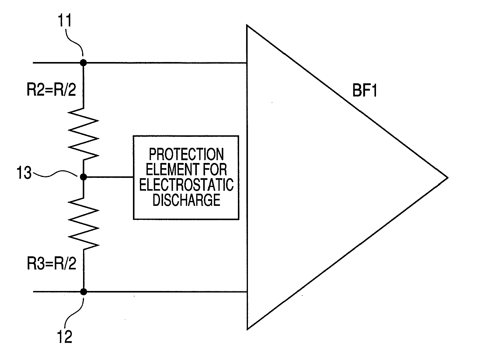
[0041]FIG. 1 is a schematic diagram of a first embodiment of a semiconductor integrated circuit device of the present invention. Differential input terminals 11 and 12 of a differential input buffer BF1 are connected to each other by a terminator R consisting of a series connection of resistances R2 and R3, and the electrostatic protection element is connected to a junction point of the resistances R2 and R3, namely, an intermediate node 13 of the terminator R. The differential input buffer BF1, the differential input terminals 11, 12, the resistances R2, R3, the intermediate node 13, and the electrostatic protection element are monolithically formed on a common semiconductor substrate, and constitute the semiconductor integrated circuit device. The electrostatic protection element is provided in order to prevent a malfunction from arising in the differential input buffer BF1 by electrostatic noises originating in the differential terminals 11, 12, for example, when attaching the se...

second embodiment

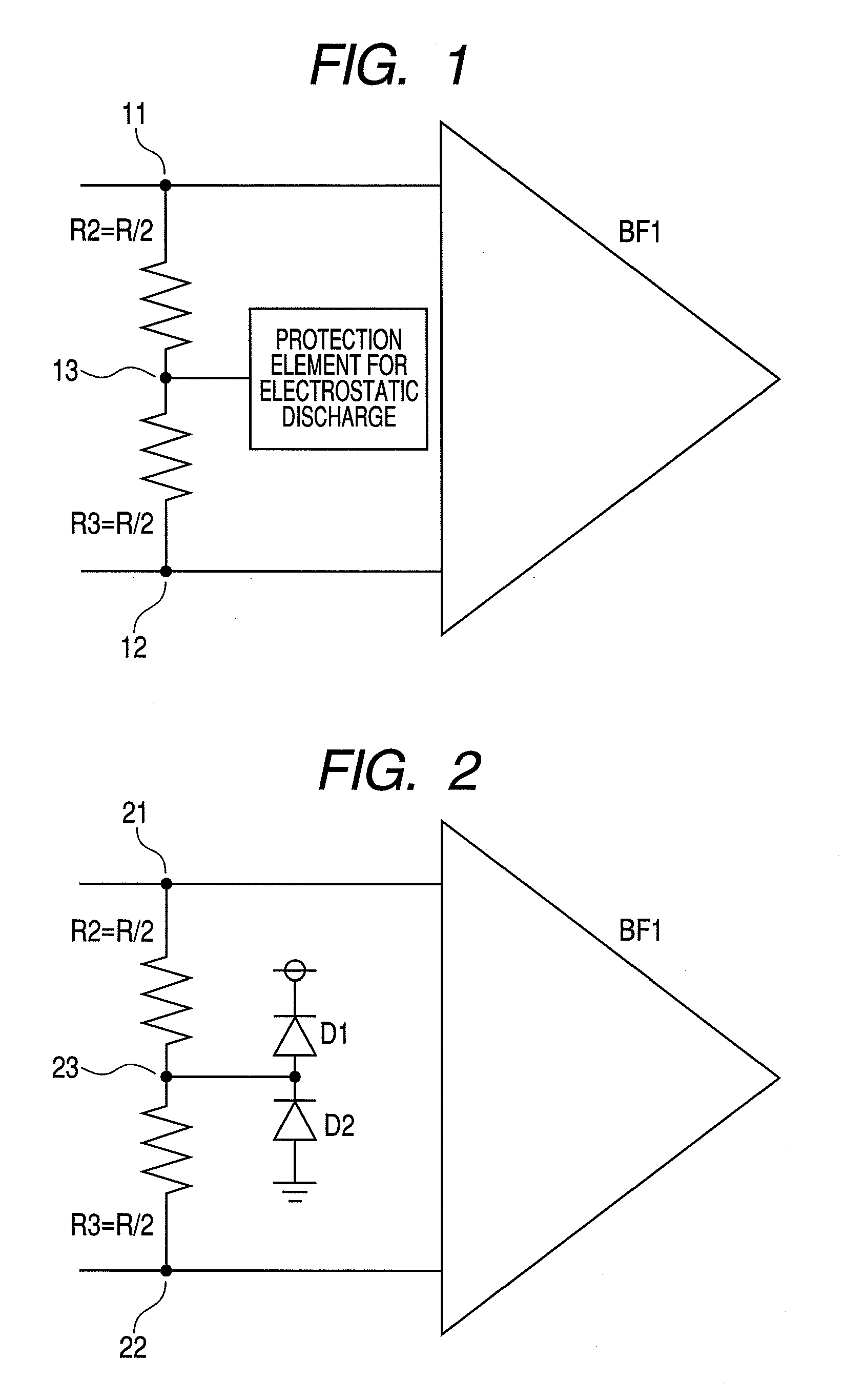
[0044]FIG. 2 is a schematic diagram of a second embodiment of the semiconductor integrated circuit device of the present invention. This embodiment is an example of the first embodiment in which diodes are used as the electrostatic protection element therein. Differential input terminals 21 and 22 of the differential input buffer BF1 are connected with each other by the terminator R consisting of a series connection of the resistances R2 and R3, and an anode side of a diode D1 and a cathode side of a diode D2 are commonly connected to the junction point of the resistances R2 and R3, namely, an intermediate node 23 of the terminator R. The two diodes D1, D2 function as the electrostatic protection element by being commonly connected to the intermediate node 23. The differential input buffer BF1, the differential input terminals 21, 22, the resistances R2, R3, the intermediate node 23 and the diodes D1, D2 are monolithically formed on a common semiconductor substrate, and constitute t...

third embodiment

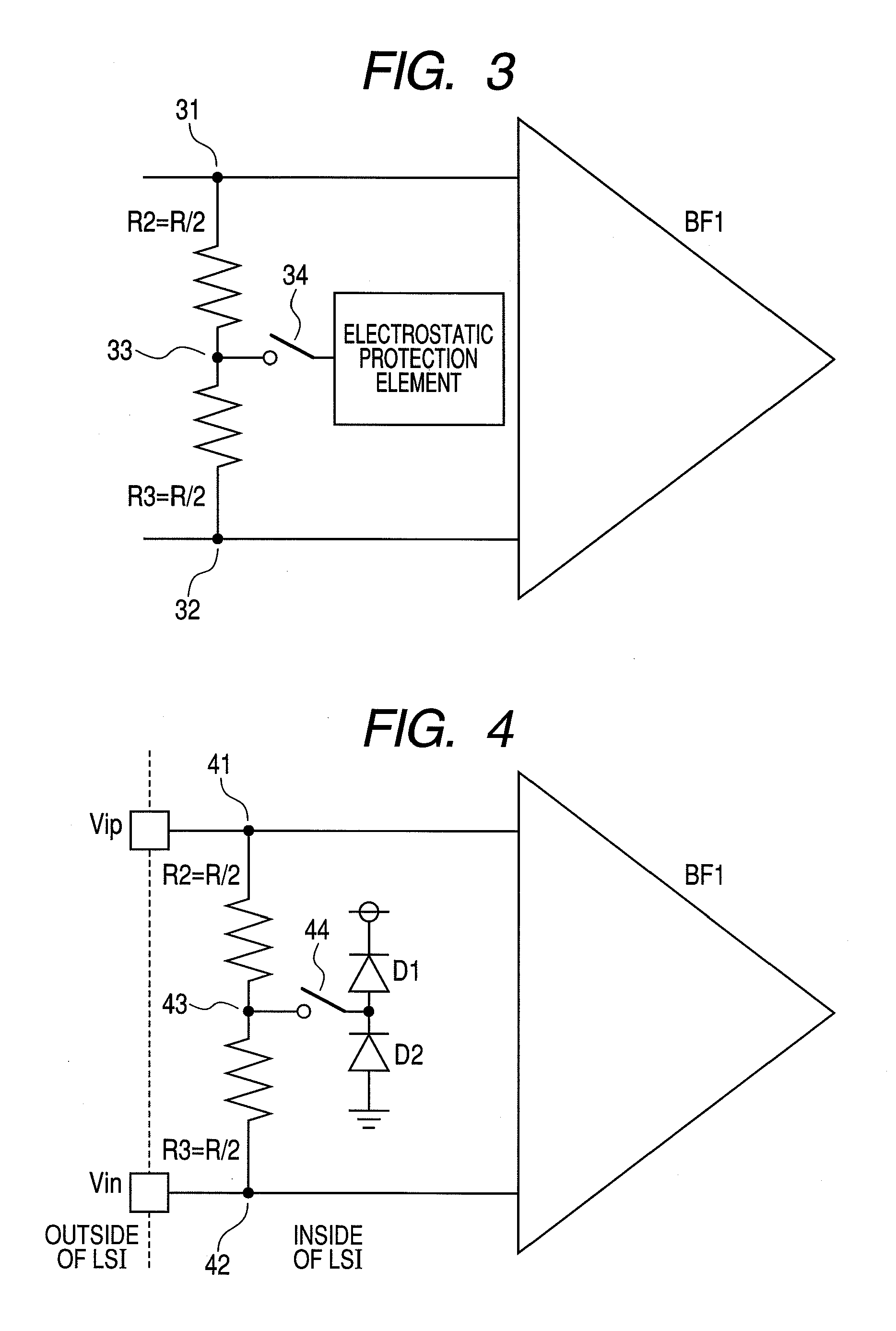
[0047]FIG. 3 is a schematic diagram of a third embodiment of the semiconductor integrated circuit device of the present invention. This embodiment is an embodiment having a configuration capable of separating the electrostatic protection element that gives the large input load at the time of actual operation in order to attain further speed enhancement from the first embodiment. Differential input terminals 31 and 32 of the differential input buffer BF1 are connected to each other by the terminator R consisting of the series connection of the resistances R2 and R3, and the electrostatic protection element is connected to the junction point of the resistances R2 and R3, namely, an intermediate node 33 of the terminator R through a switch 34. The differential input buffer BF1, the differential input terminals 31, 32, the resistances R2, R3, the intermediate node 33, the switch 34, and the electrostatic protection element are monolithically formed on a common semiconductor substrate, a...


PUM


Abstract

A semiconductor integrated circuit device supports maintenance of a signal transfer frequency and waveform quality and electrostatic protection, and also suppresses expansion of a chip area. In order to maintain the signal transfer frequency and the waveform quality as well as to keep an effect of the electrostatic protection, and simultaneously to protect a differential input pair by a single electrostatic protection element and to attain area superiority, the electrostatic protection element that is arbitrarily separable is disposed at a middle point of a terminator.

Description

CLAIM OF PRIORITY[0001]The present application claims priority from Japanese patent application JP 2009-080872 filed on Mar. 30, 2009, the content of which is hereby incorporated by reference into this application.FIELD OF THE INVENTION[0002]The present invention relates to a signal transfer technology and a semiconductor integrated circuit implementing technology and, more specifically, to a technology of a method for disposing and separating an electrostatic protection element in differential high-speed terminals that are effective in applying it in a field that requires compatibility between electrostatic protection at the time of assembly and maintenance of a signal transfer frequency band and quality of a propagation waveform into the inside of a LSI at the time of actual use.BACKGROUND OF THE INVENTION[0003]Conventionally, in order to realize compatibility between the electrostatic protection at the time of manufacture and the maintenance of the signal transfer frequency band ...

Claims


Application Information

Patent Timeline
Patent Type & Authority Applications(United States)
IPC IPC(8): H02H9/00
CPCH01L27/0255H03F2200/444H03F3/45475H03F1/52
Inventor UTAGAWA, YOSHIYUKIYAMASHITA, TAKEO
Owner HITACHI LTD
Why Eureka
Try Eureka