Image processing device, imaging device, evaluation device, image processing method, and optical system evaluation method

a technology of image processing and imaging device, applied in the field of image processing device, imaging device, evaluation device, image processing method, optical system evaluation method, can solve the problems of film generating unnecessary diffracted light, reducing the modulation transfer function characteristics, and achieving high precision and degrading image quality

Active Publication Date: 2010-09-30
PANASONIC CORP
View PDF27 Cites 16 Cited by
  • Summary
  • Abstract
  • Description
  • Claims
  • Application Information

AI Technical Summary

Benefits of technology

[0050]According to the present invention, it is possible to correct the image with degraded image quality due to the unnecessary diffracted light generated in the optical system including the diffractive optical element, and to correct the image at high precision regardless of the shape of the unnecessary diffracted light image.

Problems solved by technology

As a result, when a lens used for imaging wide wavelength band (for example, visible light with wavelength approximately from 400 nm to 700 nm) includes a diffractive optical element, unnecessary diffracted light is generated.
Subsequently, the generated unnecessary diffracted light appears as flair or a ghost and degrades an image, or reduces the modulation transfer function (MTF) characteristics.
However, even the diffractive optical element with the protective film generates the unnecessary diffracted light because of insufficiently transcribed diffraction grating at the time of forming, or displaced refractive index adjustment of the base material and the protective film material.
Furthermore, even if the diffraction efficiency is high, an absolute luminance value of the unnecessary diffracted light is large when capturing a very brightly shining light source as the object.
In other words, the degraded image quality due to the unnecessary diffracted light becomes a problem particularly when there is a large contrast between the object and the area around the object when a bright object such as a light is captured in a dark background such as nighttime scenery.

Method used


Image

  • Image processing device, imaging device, evaluation device, image processing method, and optical system evaluation method
  • Image processing device, imaging device, evaluation device, image processing method, and optical system evaluation method
  • Image processing device, imaging device, evaluation device, image processing method, and optical system evaluation method

Examples


embodiment 1

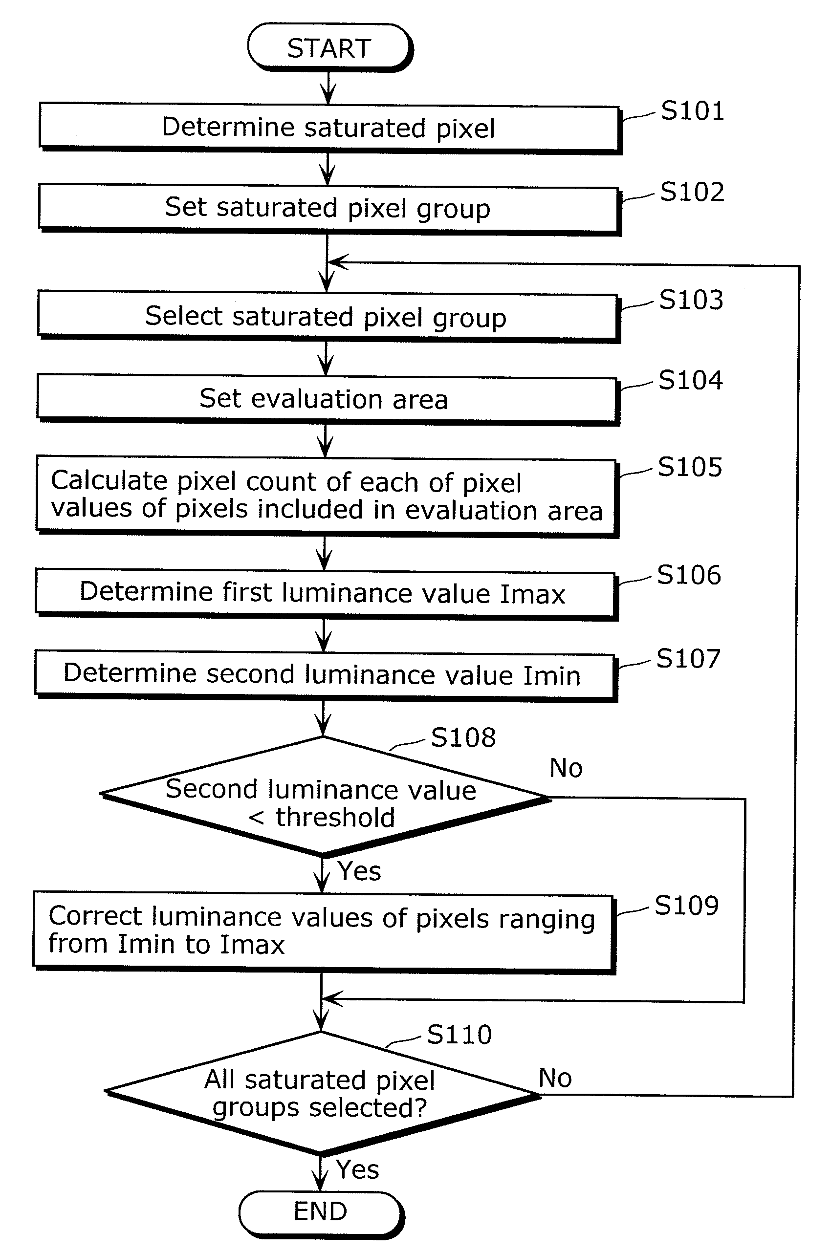
[0068]An imaging device according to Embodiment 1 of the present invention shall be described hereafter with reference to the drawings.

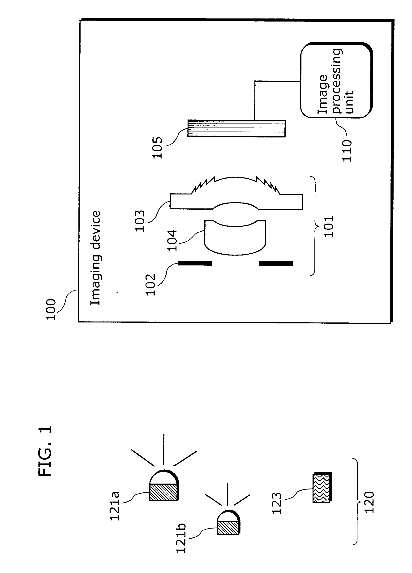
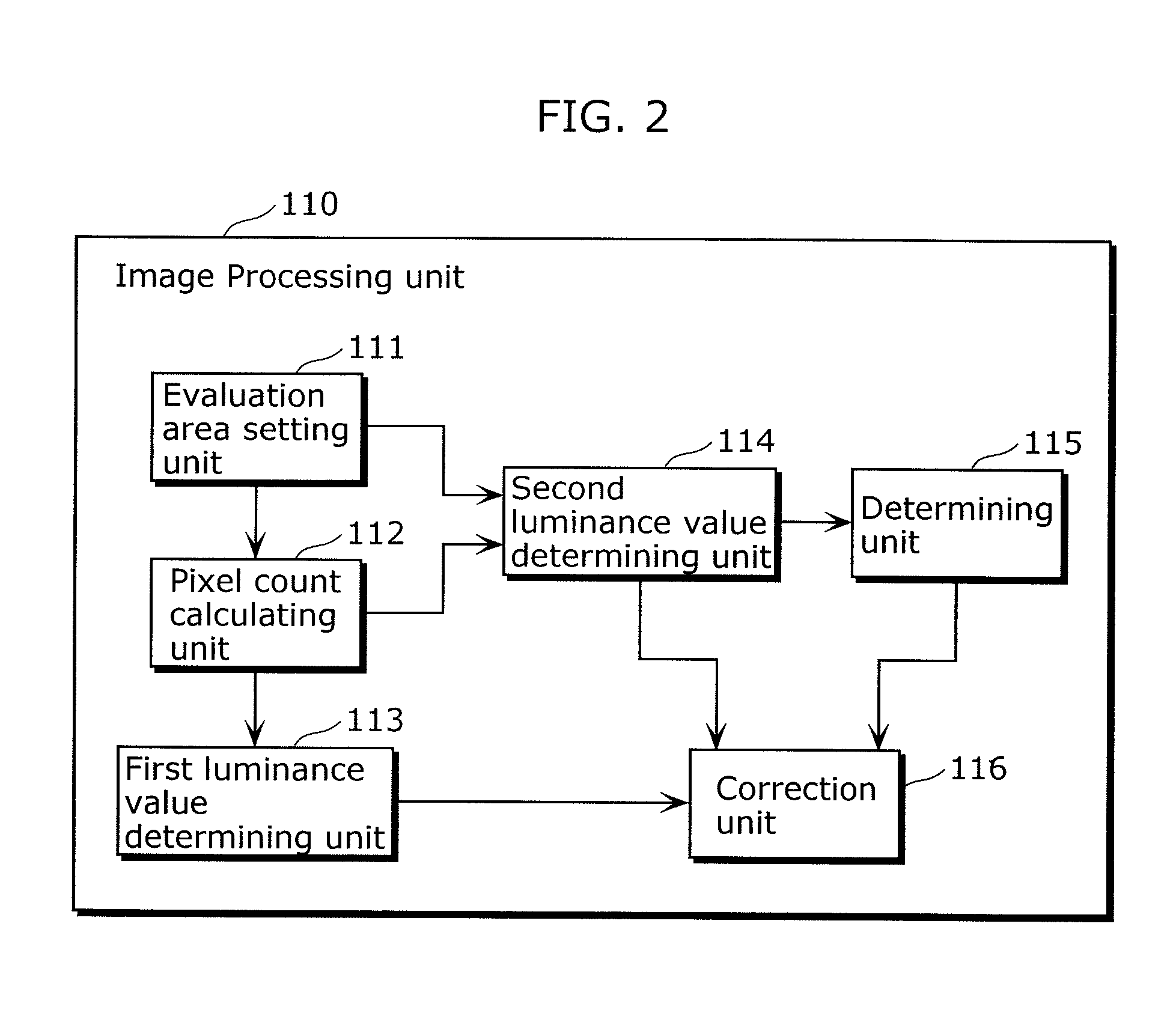
[0069]FIG. 1 is a diagram illustrating a structure of an imaging device 100 according to Embodiment 1 of the present invention. As shown in FIG. 1, the imaging device 100 includes an optical system 101, an imaging element 105 and an image processing unit 110.

[0070]The optical system 101 includes a stop 102, a diffractive optical element 103, and a refractive optical element 104. The number of diffractive optical element 103 and refractive optical element 104 included in the optical system 101 is determined according to the design purpose of the optical system. Note that, the optical system 101 in Embodiment 1 includes one diffractive optical element 103 and one refractive optical element 104. However, the optical system according to the present invention is not limited to this number. For example, the optical system 101 may include multiple diffracti...

embodiment 2

[0137]An evaluation device according to Embodiment 2 of the present invention shall be described hereafter with reference to the drawings. Note that the same reference numerals are attached to the components identical to those in the imaging device in Embodiment 1, and the description for those components are omitted.

[0138]FIG. 10 illustrates the structure of the evaluation device 200 according to Embodiment 2. As illustrated in FIG. 10, the evaluation device 200 includes a light source 221, a shielding unit 222, a movable mechanism 223, an imaging element 105 and the image processing unit 210.

[0139]The light source 221 is attached to the movable mechanism 223. The light source 221 is placed in a dark room. Placing the light source 221 in the dark room as described above can eliminate the influence of the light from a source other than the light source 221. This allows the evaluation device 200 to precisely evaluate the capability of the optical system 101 regarding the unnecessary ...

example 1

[0166]The following describes the imaging device according to Embodiment 1 of the present invention.

[0167]The imaging device 100 according to Example 1 generates a color image that has 640 by 480 pixels and 256 luminance tones. Subsequently, the imaging device 100 obtains the image in B-wavelength band by extracting the B-wavelength component from the generated color image.

[0168]The diffractive optical element L03 included in the optical system 101 of the imaging device 100 according to Example 1 includes a diffraction grating designed to have a diffraction efficiency of 100% in the G-wavelength band. Therefore, the optical system 101 in Example 1 does not have the diffraction efficiency of 100% with respect to the light in B-wavelength band. To put it differently, the optical system 101 generates unnecessary diffracted light with respect to the light in B-wavelength band.

[0169]FIG. 12 illustrates an image which is obtained by cutting an image in B-wavelength band captured by an ima...


PUM


Abstract

An image processing device that can highly precisely correct an image with a degraded image quality due to the unnecessary diffracted light generated in the optical system including the diffractive optical element is provided. The image processing device includes an evaluation area setting unit (111) which detects a saturated pixel having a saturated luminance value, from among pixels included in the image and to set an area in the image including the detected saturated pixel as an evaluation area, a pixel count calculating unit (112) which calculates a pixel count for each of luminance values of pixels included in the set evaluation area, a first luminance value determining unit (113) which determines a first luminance value indicating a maximum luminance of an image of the unnecessary diffracted light, based on a transition of calculated pixel counts arranged in order of luminance value, a second luminance value determining unit (114) which determines a second luminance value which is a luminance value corresponding to a background of the image, and a correction unit (116) which corrects a luminance value of a pixel of luminance lower than luminance of the first luminance value and higher than luminance of the second luminance value from among the pixels included in the evaluation area so as to lower the luminance of the pixel.

Description

TECHNICAL FIELD[0001]The present invention relates to an image processing device which corrects images with degraded image quality due to unnecessary diffracted light generated in an optical system including a diffractive optical element. The present invention further relates to an evaluation device which evaluates capability regarding the unnecessary diffracted light in the optical system including the diffracted optical element and a method for evaluating the optical system.BACKGROUND ART[0002]It is widely known that a diffractive optical element having a surface with annular diffractive grating can reduce lens aberration such as field curvature and chromatic aberration (displacement on imaging points due to wavelength). This is because the diffractive grating formed on the diffractive optical element has peculiar properties such as inverse dispersion and anomalous dispersion, and has a high capability for correcting chromatic aberrations. The optical system including a diffractiv...

Claims


Application Information

Patent Timeline
Patent Type & Authority Applications(United States)
IPC IPC(8): G06K9/40
CPCG06T5/009H04N5/3572H04N1/4074G06T5/40H04N25/61
Inventor ANDO, TAKAMASAKORENAGA, TSUGUHIRO
Owner PANASONIC CORP
Why Eureka
Try Eureka