Method for optical proximity correction

Inactive Publication Date: 2010-09-30
SK HYNIX INC
View PDF3 Cites 6 Cited by
  • Summary
  • Abstract
  • Description
  • Claims
  • Application Information

AI Technical Summary

Benefits of technology

[0022]Preferably, the reflecting the offset includes adding or subtracting the offset to or from the CD of the peculiar pattern. According to the present invention, in case of a pattern to which a

Problems solved by technology

However, these sources and shorter wavelengths do cause a number of difficulties in patterning in accordance to a design layout feature.
As a result the pattern printed out on the resultant wafer may become unacceptably distorted from the originally intended pattern.
As the patterns becomes finer, the light intensity likely increase to achieve the particular pattern which can adversely affect adjacent patterns due to the optical proximity effect where the pattern formed over the wafer has a different shape from a pattern of the layout on the design.
However, the contact hole pattern has a higher mask error enhancement factor so that there is a higher probability that an error can occur when only using t

Method used


Image

  • Method for optical proximity correction
  • Method for optical proximity correction
  • Method for optical proximity correction

Examples


Example

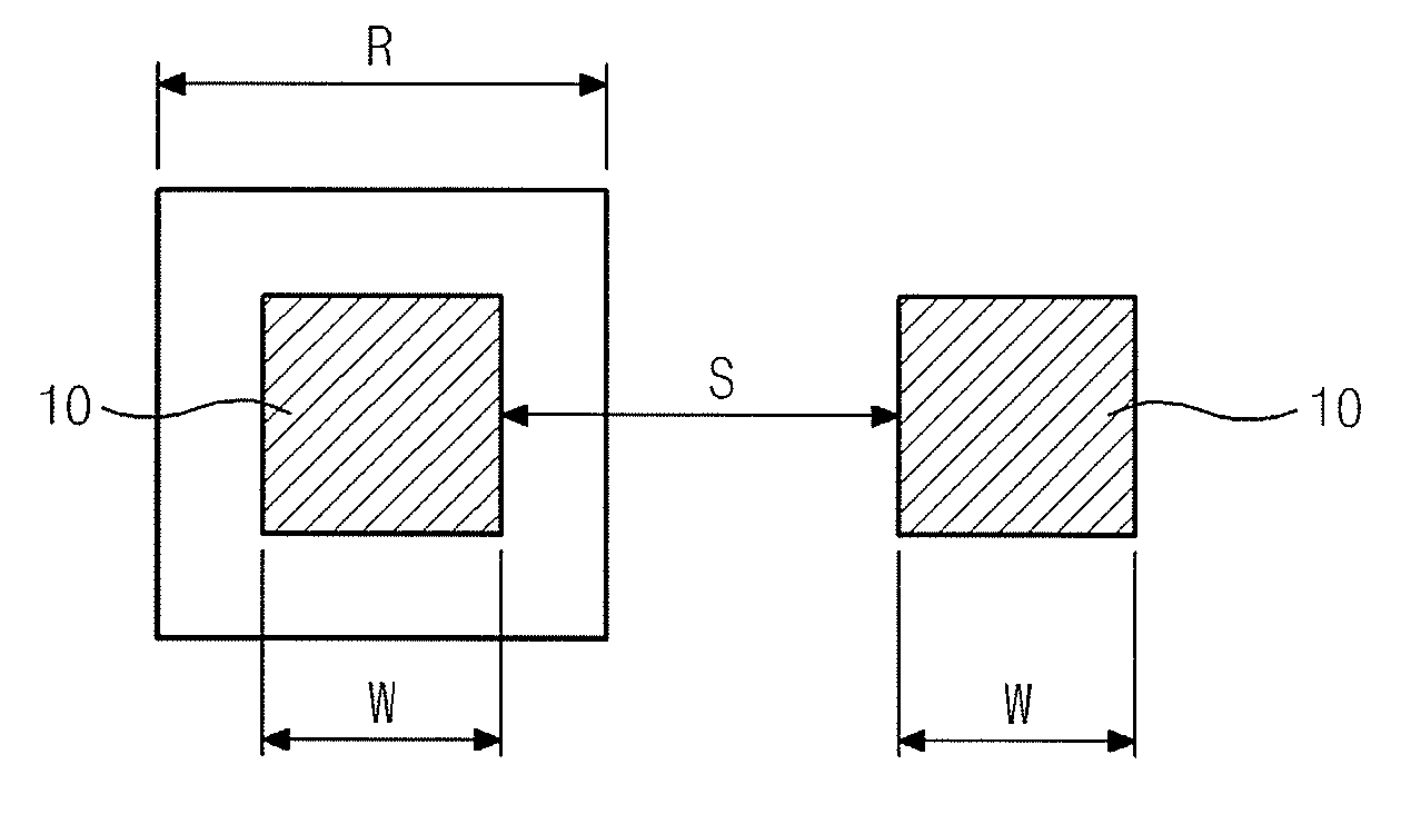
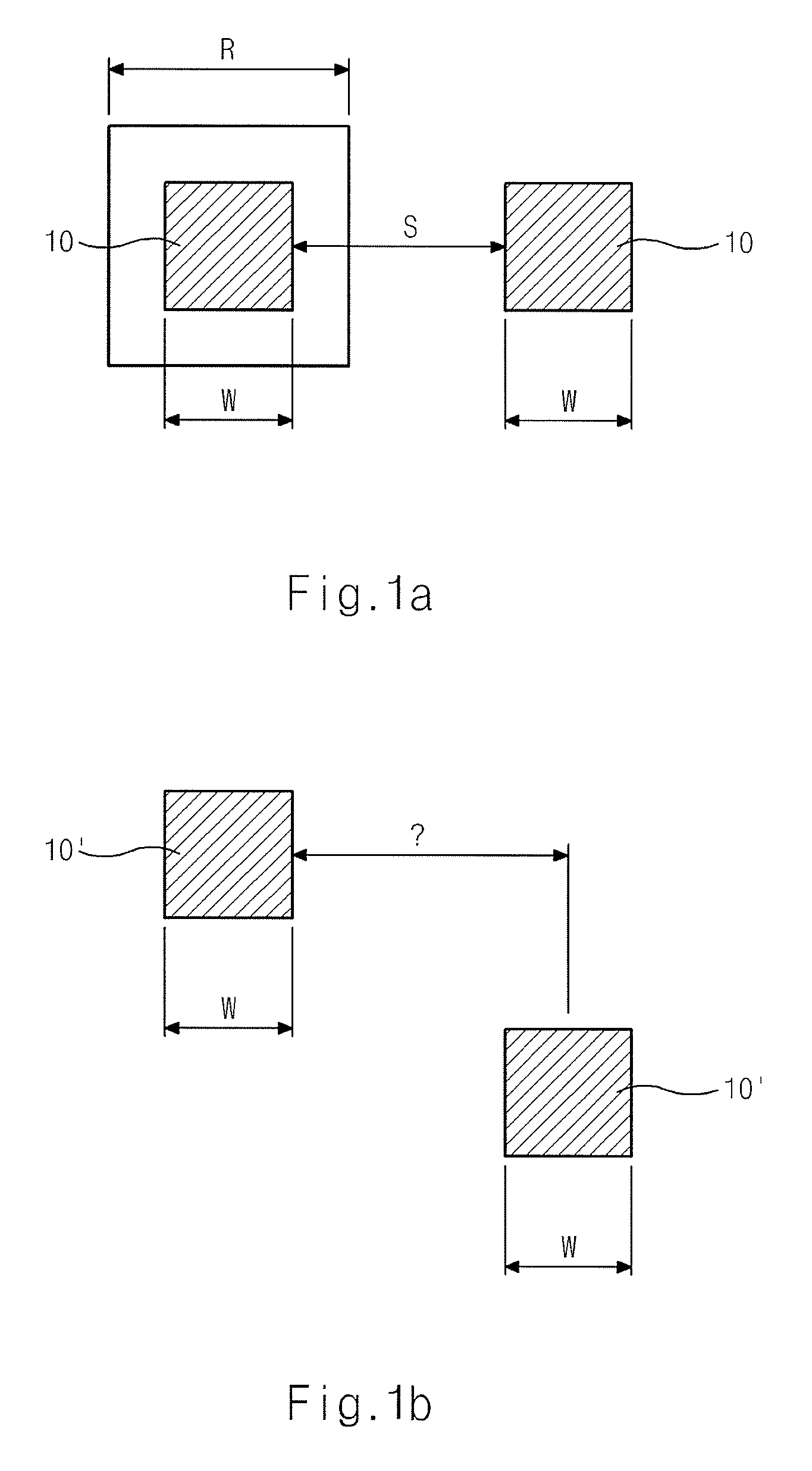
[0028]The present invention relates to an optical proximity correction method in which an optical proximity correction is performed by sorting a peculiar area from a target layout and resetting a critical dimension (CD) of a design pattern based on the sorted layout so that, in case where a pattern, such as a contact hole pattern that does not have any pattern adjacent thereto to render it difficult to apply a bias rule, the bias rule can be reflected by performing optical proximity correction, thereby improving the accuracy of the optical proximity correction. Therefore, a uniformity of a final pattern can be secured. Hereinafter, the example embodiments of the present invention will be described in detail with reference to the accompanying drawings.

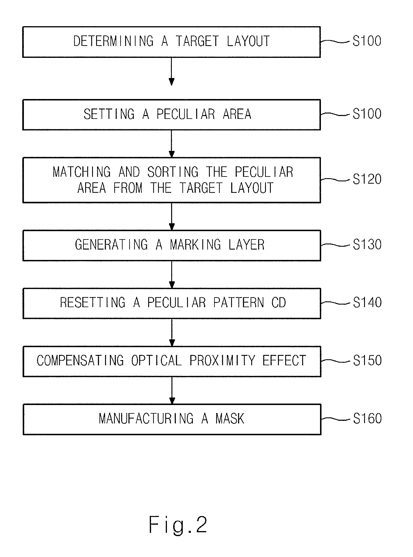
[0029]FIG. 2 is a flowchart illustrating an optical proximity correction method according to an exemplary embodiment of the present invention. FIGS. 3a through 3c illustrate a peculiar area according to an exemplary embodiment of a pres...


PUM


Abstract

Provided is a method for optical proximity correction for use in manufacturing highly resolved semiconductor chips. The method includes setting a target layout; setting a peculiar area; sorting the peculiar area from the target layout; generating a marking layer; resetting a critical dimension (CD) of a peculiar pattern; compensating an optical proximity effect; and manufacturing a mask. The method provides an improved way of improving more accurately CD uniformity by performing optical proximity correction with respect to a pattern to which a bias rule is difficult to apply due to an absence of an adjacent pattern.

Description

CROSS-REFERENCES TO RELATED APPLICATIONS[0001]The present application claims priority to Korean patent application number 10-2009-0026394, filed on Mar. 27, 2009, which is incorporated by reference in its entirety.BACKGROUND OF THE INVENTION[0002]1. Field of the Invention[0003]The present invention relates to an optical proximity correction method, and more particularly, to an optical proximity correction method for making a contact hole pattern to which a bias rule is difficult to apply.[0004]2. Description of the Related Art[0005]As the demands for increasing the integration density of semiconductor devices has continued, the design rules impose physical restraints on the methods of forming these ever refined patterns. To achieve this end of producing ever smaller patterns, shorter wavelength from exposure sources have been exploited. However, these sources and shorter wavelengths do cause a number of difficulties in patterning in accordance to a design layout feature. As a result...

Claims


Application Information

Patent Timeline
IPC IPC(8): G03F1/00
CPCG03F1/70G03F1/36
Inventor KIM, CHEOL KYUN
Owner SK HYNIX INC
Why Eureka
Try Eureka