Inductance part and method for manufacturing the same

a technology of inductance parts and manufacturing methods, applied in the field of inductance parts, can solve the problems of limitations of conventional methods in miniaturizing inductance parts, and achieve the effect of high relative magnetic permeability

Active Publication Date: 2010-10-07
PANASONIC CORP
View PDF11 Cites 43 Cited by
  • Summary
  • Abstract
  • Description
  • Claims
  • Application Information

AI Technical Summary

Benefits of technology

[0009]The present invention has an object of providing an inductance part which is reduced in size by increasing the filling factor of metal magnetic powder in a magnetic body, and a method for manufacturing the inductance part.
[0011]With this structure, the magnetic body has a high relative magnetic permeability, thereby achieving the miniaturization of the inductance part.

Problems solved by technology

Therefore, the conventional method has limitations in miniaturizing inductance parts by increasing the filling factor of the metal magnetic powder in magnetic body 4.

Method used


Image

  • Inductance part and method for manufacturing the same
  • Inductance part and method for manufacturing the same
  • Inductance part and method for manufacturing the same

Examples


first exemplary embodiment

[0057]An inductance part of the present invention will be described as follows as a first exemplary embodiment with reference to drawings.

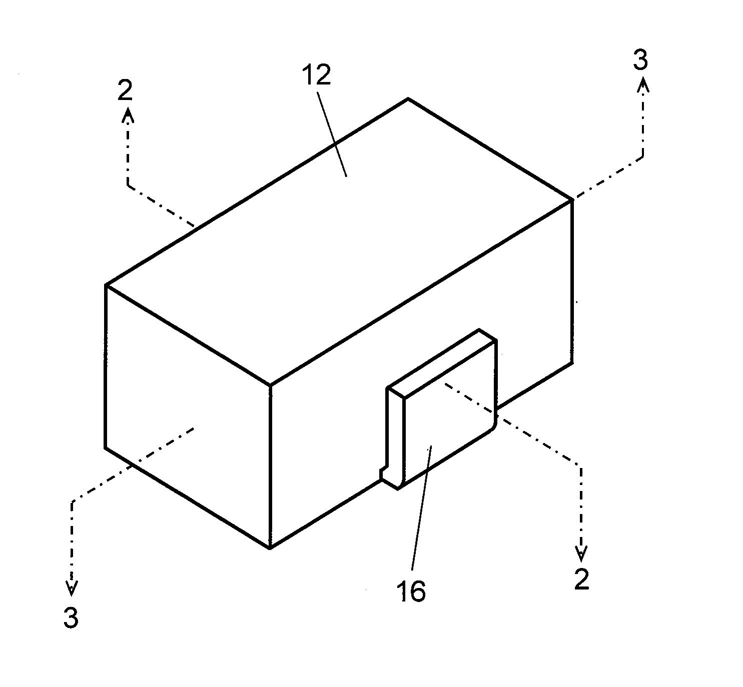
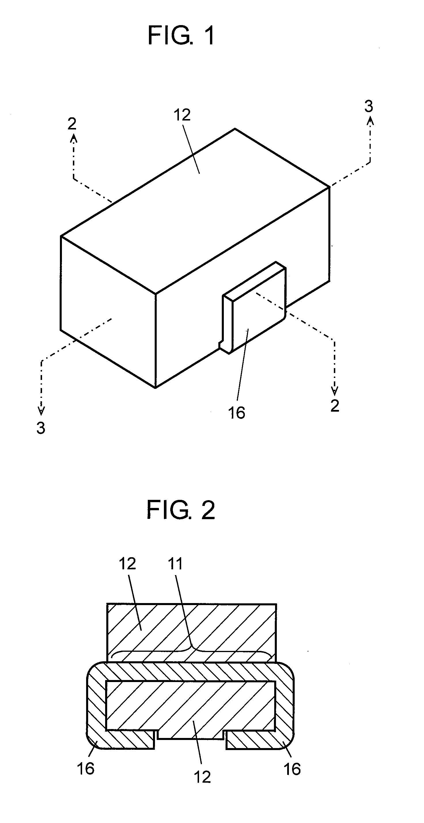
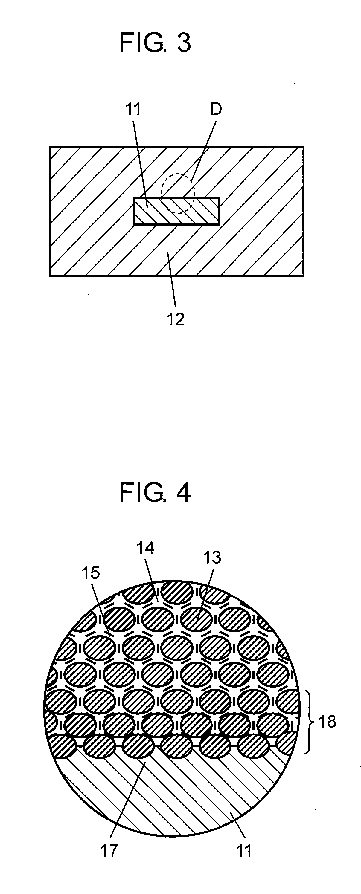
[0058]FIG. 1 is a perspective view of an inductance part of the first exemplary embodiment. FIG. 2 is a sectional view of FIG. 1 taken along a line 2-2. FIG. 3 is a sectional view of FIG. 1 taken along a line 3-3. FIG. 4 is an enlarged schematic diagram of a part D of FIG. 3.

[0059]In FIGS. 1 to 4, the inductance part includes coiled conductor 11, which is formed from a metal conductor such as a copper plate. Coiled conductor 11 is formed in a single layer by linearly punching a metal plate, and is not provided on its surface with an insulating film. Coiled conductor 11 may be made of any material having excellent conductivity such as a copper plate having a Vickers hardness of 50 to 150 (HV).

[0060]The inductance part further includes magnetic body 12, which is formed by pressure-molding a mixture of metal magnetic powder 13 and bonding material 14...

second exemplary embodiment

[0087]The inductance part of the present invention will be described as follows as a second exemplary embodiment with reference to drawings. Like components are labeled with like reference numerals with respect to the first exemplary embodiment, and these components are not described again in detail.

[0088]FIG. 6 is a perspective view of an inductance part of the second exemplary embodiment. FIG. 7 is a sectional view of FIG. 6 taken along a line 7-7. As shown in FIGS. 6 and 7, in the inductance part of the second exemplary embodiment, magnetic body 12 includes upper surface portion 21 above coiled conductor 11, lower surface portion 22 below coiled conductor 11, and intermediate portion 23 besides coiled conductor 11. Upper and lower surface portions 21 and 22 have a higher density than intermediate portion 23. Magnetic body 12 has intermediate portion's thickness 26, which is larger than upper surface portion's thickness 24 and lower surface portion's thickness 25.

[0089]In the cros...

third exemplary embodiment

[0095]The inductance part of the present invention will be described as follows as a third exemplary embodiment with reference to drawings. Like components are labeled with like reference numerals with respect to the first exemplary embodiment, and these components are not described again in detail.

[0096]FIG. 9 is a perspective view of an inductance part of the third exemplary embodiment. FIG. 10 is a sectional view of FIG. 9 taken along a line 10-10. In FIGS. 9 and 10, coiled conductor 11 includes bias portions 29 at both ends thereof connected to terminals 16. Bias portions 29 each include upward-bent part 27 which is bent upward and laterally-bent part 28 which is bent laterally. Coiled conductor 11 has its center located at the substantial center of the upper and lower surfaces of magnetic body 12. Terminals 16 are biased toward the top of the side surfaces of magnetic body 12 and derived from coiled conductor 11.

[0097]The shape of coiled conductor 11 will be described in greate...


PUM

PropertyMeasurementUnit
temperatureaaaaaaaaaa
frequencyaaaaaaaaaa
pressureaaaaaaaaaa

Abstract

Disclosed is an inductance part including a coiled conductor formed from a metal conductor, a magnetic body formed by pressure-molding a mixture of metal magnetic powder and bonding material in such a manner that the coiled conductor is embedded in the mixture, and a terminal derived from the coiled conductor. The coiled conductor is formed in a single layer with no insulating film on its surface. The metal magnetic powder of the magnetic body penetrates into the surface of the coiled conductor so as to make the filling factor of the metal magnetic powder in the magnetic body not less than 80% by volume.

Description

TECHNICAL FIELD[0001]The present invention relates to inductance parts used particularly as power choke coils in various electronic devices, and a method for manufacturing the inductance parts.BACKGROUND ART[0002]Power supply circuits used in computers and the like in recent years operate in a high-frequency domain of 300 kHz to 1 MHz. Inductance parts used in these power supply circuits are required to have an inductance value of about 1 pH and a DC resistance of several milliohms and also to correspond to a large current of over ten amperes. To meet these demands, there have been proposed inductance parts having dimensions of about 10 mm wide, 10 mm deep, and 4 mm high, and having a so-called compressed powder magnetic core. The compressed powder magnetic core is formed by embedding a coil in metal magnetic powder having a high saturation magnetic flux density at a high-frequency current.[0003]A conventional inductance part will be described as follows with reference to drawings.[...

Claims


Application Information

Patent Timeline
Patent Type & Authority Applications(United States)
IPC IPC(8): H01F5/00H01F41/02H01F3/08H01F27/24
CPCH01F3/10H01F17/04H01F17/06H01F27/2847Y10T29/49076H01F41/005H01F41/0246H01F2017/048H01F27/292
Inventor SHIMOMURA, SATORUTAKAGI, KIYOSHIOONISHI, KAZUAKI
Owner PANASONIC CORP
Why Eureka
Try Eureka