Substrate reactor with adjustable injectors for mixing gases within reaction chamber

a technology of reactant and injector, which is applied in the direction of coating, chemical vapor deposition coating, metallic material coating process, etc., can solve the problems of premature reaction reaction reaction, high cost, and low quality and yield

Active Publication Date: 2010-10-07
ASM IP HLDG BV
View PDF102 Cites 372 Cited by
  • Summary
  • Abstract
  • Description
  • Claims
  • Application Information

AI Technical Summary

Problems solved by technology

However, existing processes tend to produce films that are non-uniform across the surface of a wafer, resulting in lower quality and yield, and thus, higher costs.
However, strong exothermic reactions have been observed, potentially leading to premature reactant breakdown, damage to the gas intermixing tank, combustion, and substrate contamination.
Other selective deposition chemistries are also subject to excessive reactivity.

Method used


Image

  • Substrate reactor with adjustable injectors for mixing gases within reaction chamber
  • Substrate reactor with adjustable injectors for mixing gases within reaction chamber
  • Substrate reactor with adjustable injectors for mixing gases within reaction chamber

Examples


Embodiment Construction

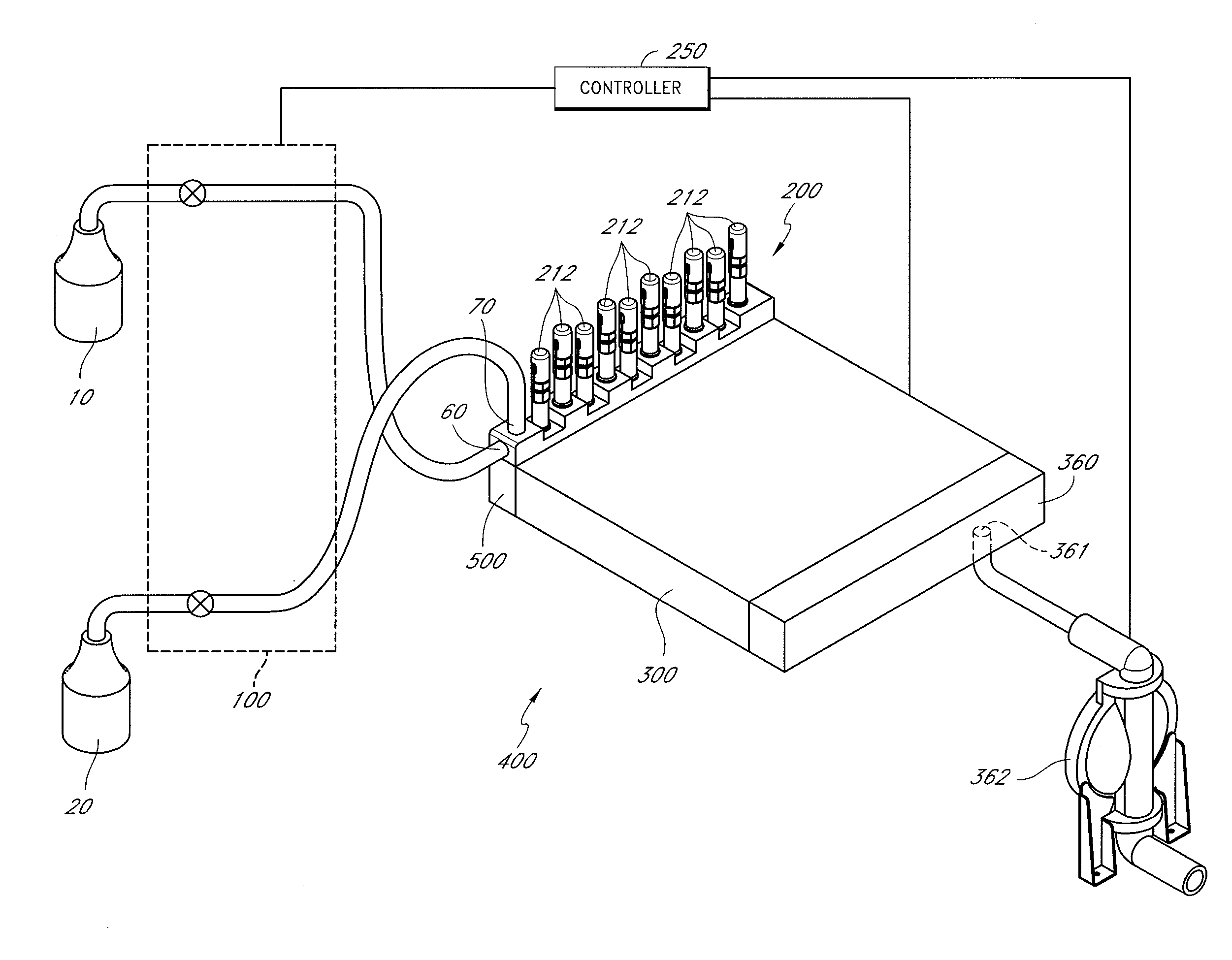
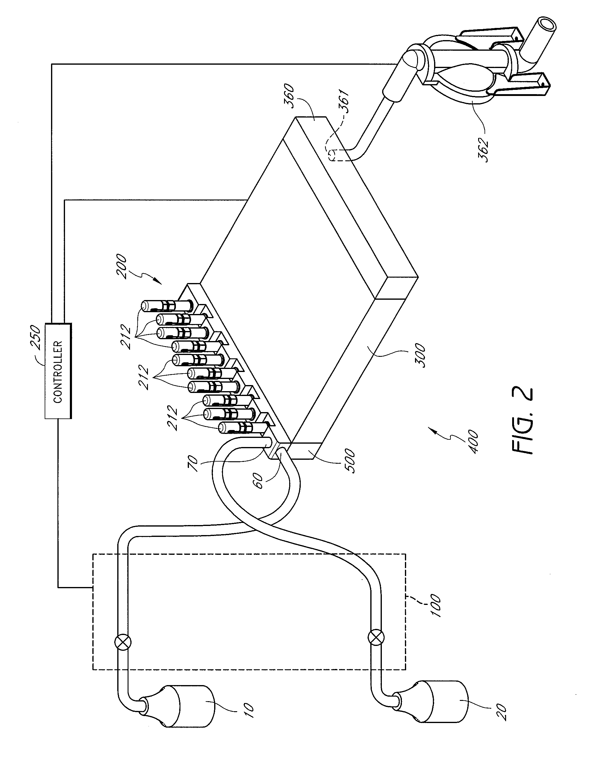
[0030]Supplying substrate processing equipment that can execute a selective deposition process and still mitigate the reactivity issues described above in the Background section may have an impact on the equipment manufacturer or user. Replacing an entire CVD processing system can be cost prohibitive, and the compatibility of a selective deposition-capable equipment design with an existing system may increase the system's footprint in a semiconductor fabrication facility. An equipment design that provides selective deposition capability must also maximize tuning capability as discussed above while providing accessibility to the equipment for the user.

[0031]In many selective deposition processes, Si-containing layers are selectively formed over single crystal semiconductor materials while minimizing and more preferably avoiding deposition over adjacent dielectrics. Examples of dielectric materials include silicon dioxide (including low dielectric constant forms such as carbon-doped o...


PUM

PropertyMeasurementUnit
diametersaaaaaaaaaa
diametersaaaaaaaaaa
diametersaaaaaaaaaa

Abstract

Methods and apparatuses for separately injecting gases into a reactor for a substrate processing system. The flow profiles of the gases are controlled with two or more sets of adjustable gas flow injectors. The methods are particularly useful for selective deposition of gases in a CVD system using volatile combinations of precursors and etchants. In either case, the gases are provided along separate flow paths that intersect in a relatively open reaction space, rather than in more confined upstream locations.

Description

BACKGROUND OF THE INVENTION[0001]1. Field of the Invention[0002]This application relates generally to processing substrates. More particularly, this application relates to the deposition of films onto a substrate and equipment configured for the same.[0003]2. Description of the Related Art[0004]As is well known, substrate processing methods and equipment are often employed for semiconductor processing and for the fabrication of integrated circuits, which entails particularly stringent quality demands, but such processing is also employed in a variety of other fields. For example, semiconductor processing techniques are often employed in the fabrication of flat panel displays using a wide variety of technologies and in the fabrication of microelectromechanical systems (MEMS).[0005]A variety of methods are used in substrate processing to deposit materials onto surfaces. For example, one of the most widely used methods in the semiconductor manufacturing industry is chemical vapor depos...

Claims


Application Information

Patent Timeline
Patent Type & Authority Applications(United States)
IPC IPC(8): H01L21/20C23C16/455
CPCC23C16/04C23C16/45574C23C16/45563C23C16/45504
Inventor AGGARWAL, RAVINDERCONNER, RANDDISANTO, JOHNALEXANDER, JAMES A.
Owner ASM IP HLDG BV
Why Eureka
Try Eureka