Lithography method and apparatus for semiconductor device fabrication

Active Publication Date: 2010-10-07
TAIWAN SEMICON MFG CO LTD
View PDF4 Cites 6 Cited by
  • Summary
  • Abstract
  • Description
  • Claims
  • Application Information

AI Technical Summary

Benefits of technology

[0004]In another embodiment, a lithography system is provided. The system includes a radiation source for providing a radiation energy and an imaging system configured to direct the radiation energy onto a substrate to form an image thereon. The system further includes a first aperture operable to be incorporated with the imaging system. The first aperture has a first pair of radiation-transmitting regions positioned along a first diametrical axis and a second pair of radiation-transmitting regions positioned along a second diametrical axis substantially perpendicular to the first diametrical axis. The first pair of radiation-transmitting regions allow a grea

Problems solved by technology

However, the process window to perform DDL may be limited.

Method used


Image

  • Lithography method and apparatus for semiconductor device fabrication
  • Lithography method and apparatus for semiconductor device fabrication
  • Lithography method and apparatus for semiconductor device fabrication

Examples


Embodiment Construction

[0011]It is understood that the following disclosure provides many different embodiments, or examples, for implementing different features of the invention. Specific examples of components and arrangements are described below to simplify the present disclosure. These are, of course, merely examples and are not intended to be limiting. In addition, the present disclosure may repeat reference numerals and / or letters in the various examples. This repetition is for the purpose of simplicity and clarity and does not in itself dictate a relationship between the various embodiments and / or configurations discussed.

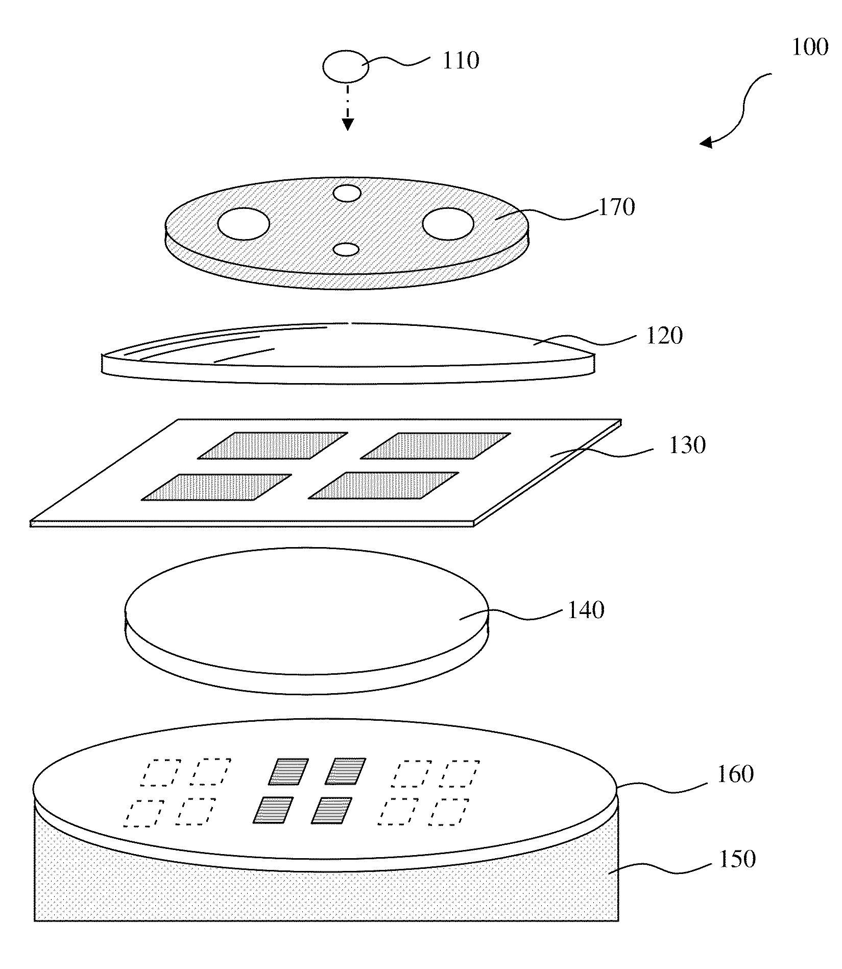
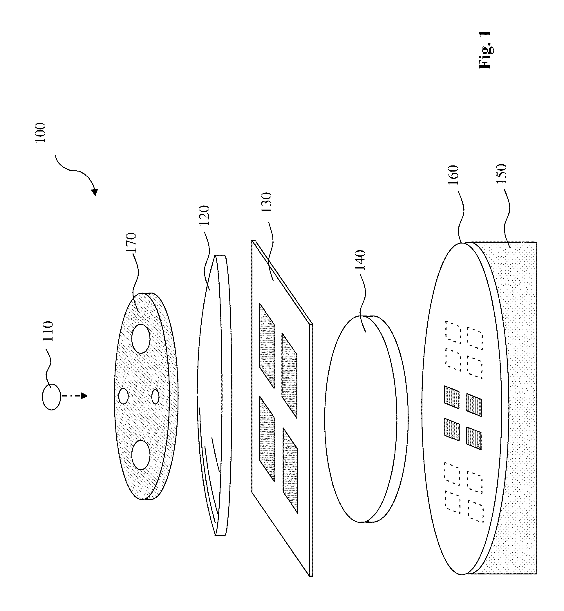
[0012]Referring to FIG. 1, in one embodiment, a lithography system 100 includes a radiation source (or source) 110. The radiation source 110 may be any suitable radiation source. For example, the source 110 may be a mercury lamp having a wavelength of 436 nm (G-line) or 365 nm (I-line); a Krypton Fluoride (KrF) excimer laser with wavelength of 248 nm; an Argon Fluoride (ArF) excim...


PUM


Abstract

Provided is a lithography system operation to include a first aperture or a second aperture. Each of the first and second apertures has two pairs of radiation-transmitting regions where one pair of radiation-transmitting regions are larger than a second pair. For an aperture, each pair of radiation-transmitting regions are on different diametrical axis. In an embodiment, one aperture is used for x-dipole illumination and the second aperture is used for y-dipole illumination.

Description

BACKGROUND[0001]Semiconductor integrated circuit (IC) technology has experienced rapid progress including the continued minimization of feature sizes and the maximization of packing density. The minimization of feature size relies on improvement in photolithography and its ability to print smaller features or critical dimensions (CD). Various techniques have been developed to enhance the resolution of optical lithography. An example of such a technique is off-axis illumination (OAI). OAI illumination may include any radiation that reduces and / or eliminates the “on-axis” (on the optical axis) component of the radiation. For OAI however, the shape and size of the illumination must be optimized for the specific pattern that is to be printed on a substrate. Another RET technique used is double dipole lithography (DDL) or double patterning which can use a strong OAI. DDL requires decomposition of patterns into a vertical pattern and a horizontal pattern, which in turn requires two (doubl...

Claims


Application Information

Patent Timeline
IPC IPC(8): H01L21/461G03F7/20G03B27/54
CPCG03B27/54H01L21/302G03B27/523G03F7/701
Inventor WANG, HSIEN-CHENGHSIEH, HUNG CHANGWANG, SHIH-CHEWU, PING CHIEHHUANG, WEN-CHUNWEN, MING-CHANG
Owner TAIWAN SEMICON MFG CO LTD
Why Eureka
Try Eureka