Unit pixel of image sensor having three-dimensional structure and method for manufacturing the same

a technology of image sensor and unit pixel, which is applied in the direction of semiconductor/solid-state device details, radiation control devices, semiconductor devices, etc., can solve the problems of difficult etching and filling, processing involved, and the likelihood of deterioration of uniformity and repeatability during aligning wafers, so as to achieve easy and precise implementation

Active Publication Date: 2010-10-14
SK HYNIX INC
View PDF3 Cites 58 Cited by
  • Summary
  • Abstract
  • Description
  • Claims
  • Application Information

AI Technical Summary

Benefits of technology

[0010]Accordingly, the present invention has been made in an effort to solve the problems occurring in the related art, and an object of the present invention is to provide a unit pixel of an image sensor having a three-dimensional structure, which can allow alignment of chips during the manufacture of an image sensor to be easily and precisely implemented with respect to sideward movement and rotation while obviating the need for a separate device for alignment, and a method for manufacturing the same.

Problems solved by technology

In the TSV process, etching and filling are difficult to conduct, and uniformity and repeatability during aligning wafers are likely to deteriorate depending upon chips or wafers.
Further, in a super via (contact) method and an infrared irradiation method, which are used in the conventional art as an alignment (arrangement) method for bonding wafers, problems are caused in that processing is involved and the precision of the alignment may be degraded.

Method used


Image

  • Unit pixel of image sensor having three-dimensional structure and method for manufacturing the same
  • Unit pixel of image sensor having three-dimensional structure and method for manufacturing the same
  • Unit pixel of image sensor having three-dimensional structure and method for manufacturing the same

Examples


Embodiment Construction

[0020]Reference will now be made in greater detail to a preferred embodiment of the invention, an example of which is illustrated in the accompanying drawings. Wherever possible, the same reference numerals will be used throughout the drawings and the description to refer to the same or like parts.

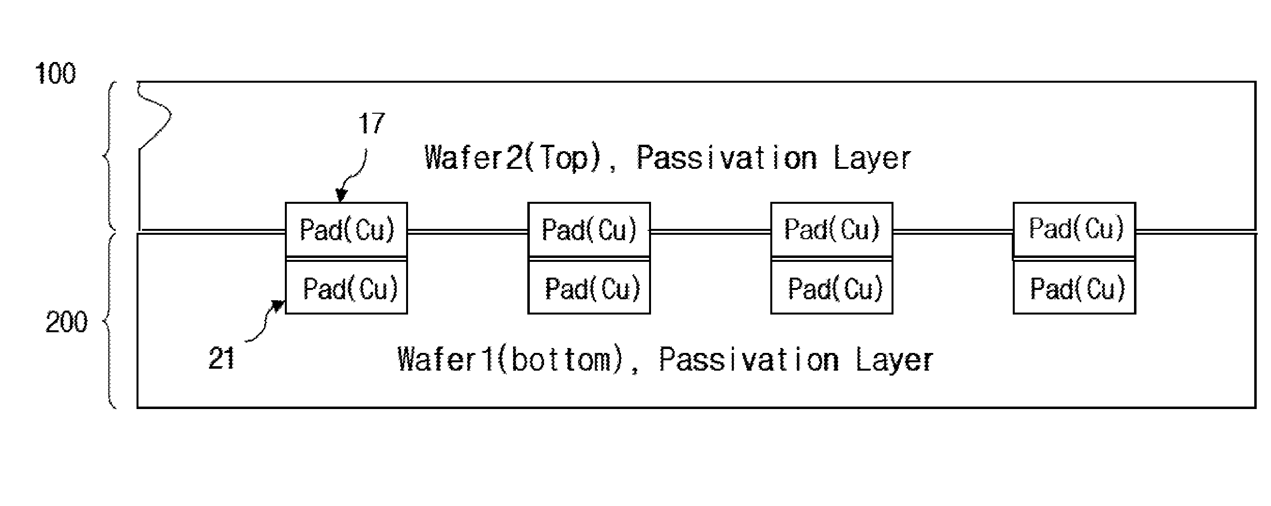
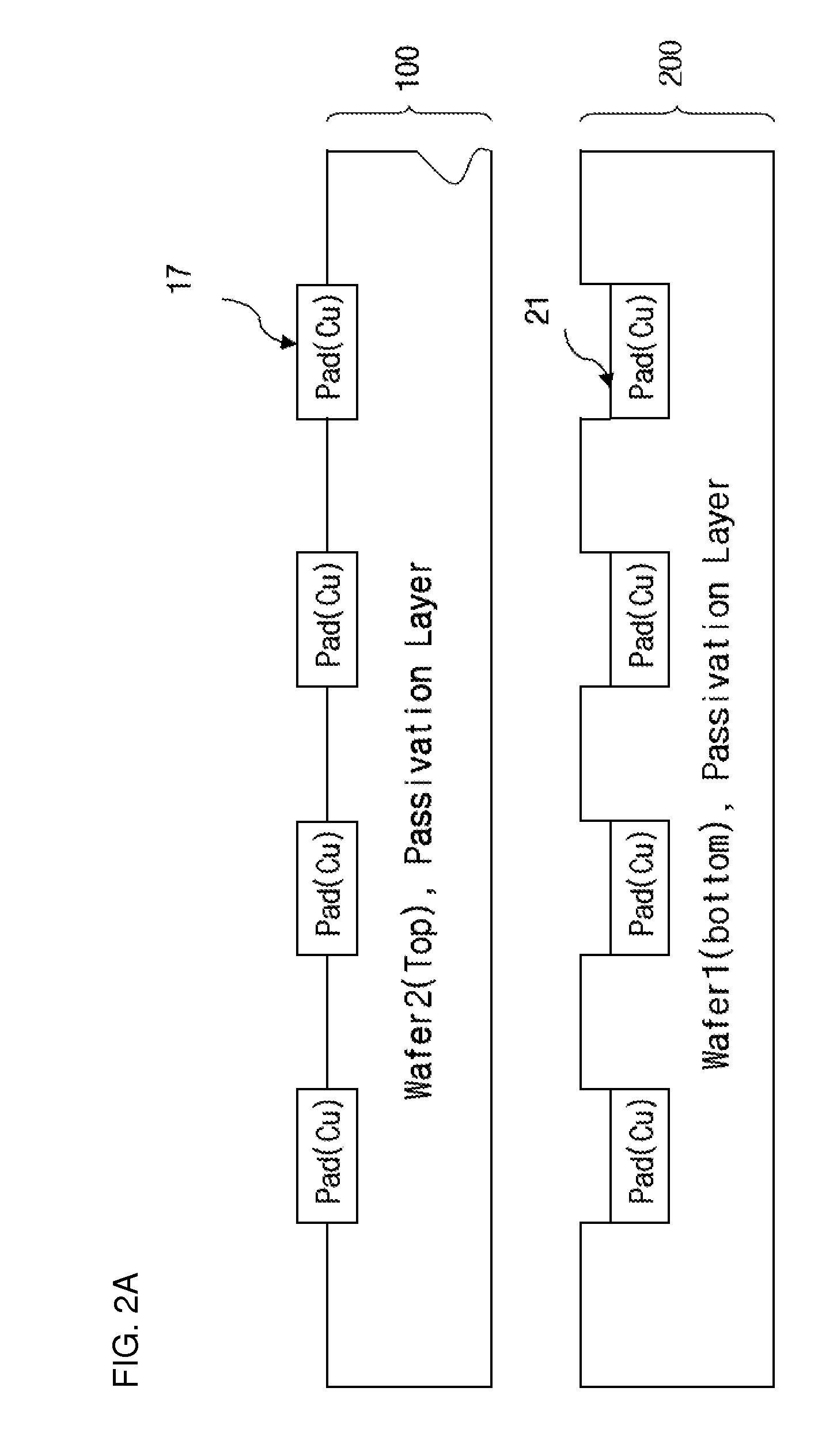
[0021]FIGS. 2a through 2c are cross-sectional views illustrating main processes associated with the alignment of wafers on which a unit pixel of an image sensor having a three-dimensional structure according to the present invention is stacked.

[0022]First, referring to FIG. 2a, electrode pads 17 and 21 are respectively formed on a first wafer 100 and a second wafer 200.

[0023]The first wafer 100 is formed with a plurality of first pads 17 which project from the upper surface of the first wafer 100 in such a way as to define a concavo-convex structure. The second wafer 200 is formed with a plurality of second pads 21 which are depressed from the upper surface of the second wafer 200 in such ...


PUM


Abstract

A unit pixel of an image sensor having a three-dimensional structure includes a first chip and a second chip which are stacked, one of the first chip and the second chip having a photodiode, and the other of the first chip and the second chip having a circuit for receiving information from the photodiode and outputting received information. The first chip includes a first pad which is projectedly disposed on an upper surface of the first chip in such a way as to define a concavo-convex structure, and the second chip includes a second pad which is depressedly disposed on an upper surface of the second chip in such a way as to define a concavo-convex structure corresponding to the concavo-convex structure of the first chip. The first chip and the second chip are mated with each other through bonding of the first pad and the second pad.

Description

BACKGROUND OF THE INVENTION[0001]1. Field of the Invention[0002]The present invention relates to a unit pixel of an image sensor, and more particularly, to a unit pixel of an image sensor having a three-dimensional structure, which has a transistor and a photodiode, and a method for manufacturing the same.[0003]2. Description of the Related Art[0004]Referring to Korean Patent No. 10-0782463 entitled[0005]“Separation type unit pixel of image sensor having 3 dimensional structure and manufacture method thereof”, in order to increase a fill factor as a ratio between the area occupied by a photodiode and the size of a pixel, a wafer, in which a photodiode is formed, and a wafer, in which other circuit components are formed, are separately manufactured and are bonded to each other by way of conductive pads. As an alignment (arrangement) method for bonding the wafers, infrared (IR) irradiation, etching and laser punching are used.[0006]FIG. 1 is a photograph showing the cross-section of a...

Claims


Application Information

Patent Timeline
Patent Type & Authority Applications(United States)
IPC IPC(8): H01L31/10
CPCH01L23/535H01L27/1464H01L24/05H01L27/14609H01L27/14632H01L27/14634H01L27/14636H01L27/14687H01L27/14689H01L27/1469H01L31/02005H01L2223/5446H01L2224/0401H01L2224/05552H01L2224/05568H01L2224/13021H01L2924/01033H01L2924/01077H01L2924/01005H01L2924/01006H01L2224/16237H01L2224/81191H01L2224/81141H01L2224/05551H01L2224/05553H01L2224/06051H01L24/03H01L24/81H01L2924/00012H01L2924/12042H01L2924/12043H01L2224/8034H01L2224/80141H01L2224/03616H01L2224/08147H01L2924/00H01L27/146H04N25/00
Inventor AHN, HEUI-GYUN
Owner SK HYNIX INC
Why Eureka
Try Eureka