[0071]According to the second aspect of the present invention, when generating the voltage which is to be supplied to the control terminal of the output-side switching element in order to turn ON the output-side switching element, the boosted voltage is supplied from the main boosting capacitor to the control-boosting capacitor via a control-boosting switching element. In this process, the control terminal of the control-boosting switching element is supplied with a voltage which is higher than the boosted voltage by at least the
threshold voltage of the control-boosting switching element. This eliminates
voltage drop by threshold value in the control-boosting switching element, and it is now possible to reliably generate a voltage which is higher than the boosted voltage by at least the
threshold voltage of the output-side switching element as a voltage that is to be supplied to the control terminal of the output-side switching element when turning ON the output-side switching element. The arrangement more reliably removes influences of
voltage drop by threshold value on the boosted supply voltage which is outputted from the power supply circuit.
[0072]According to the third aspect of the present invention, two
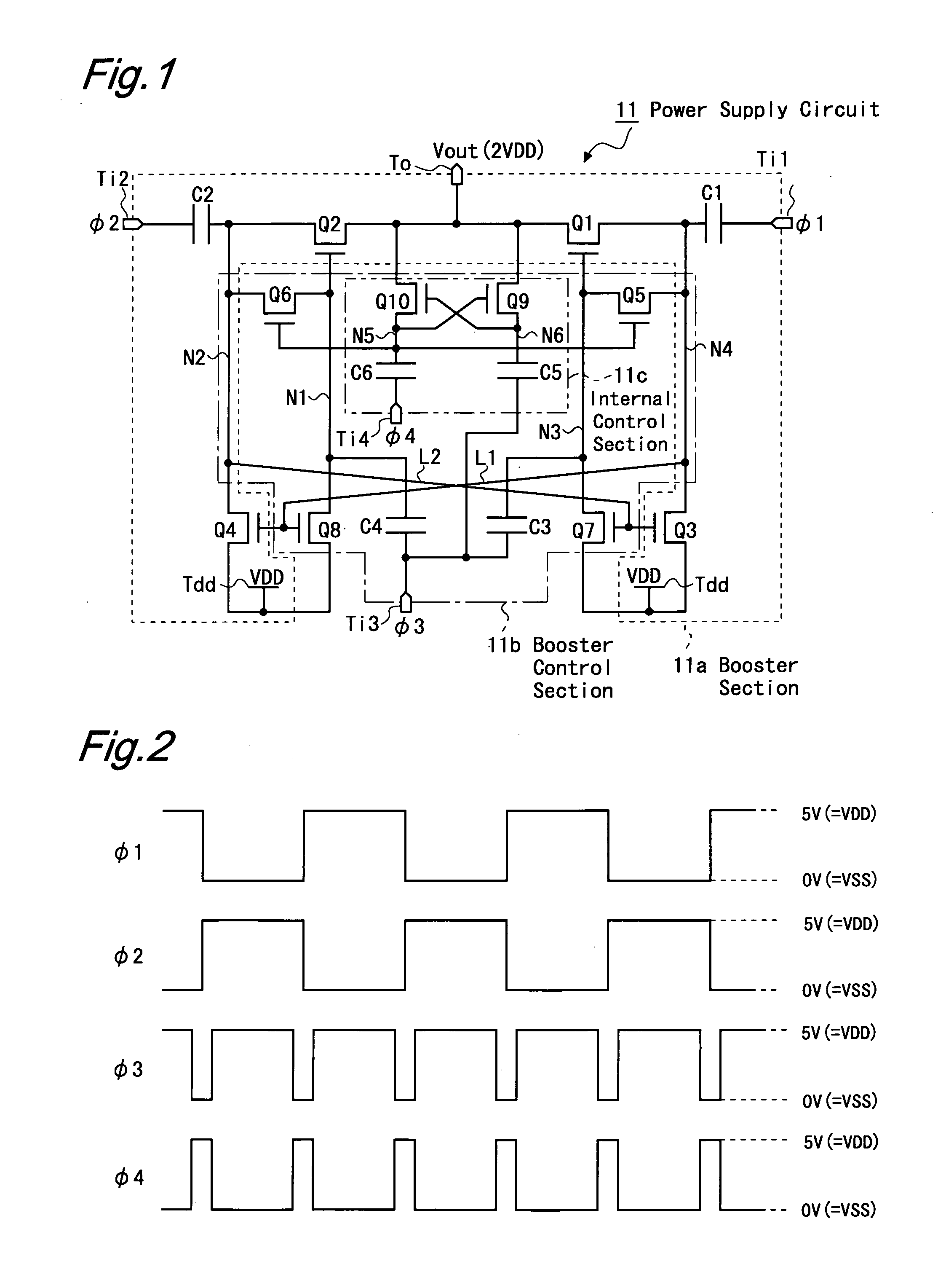
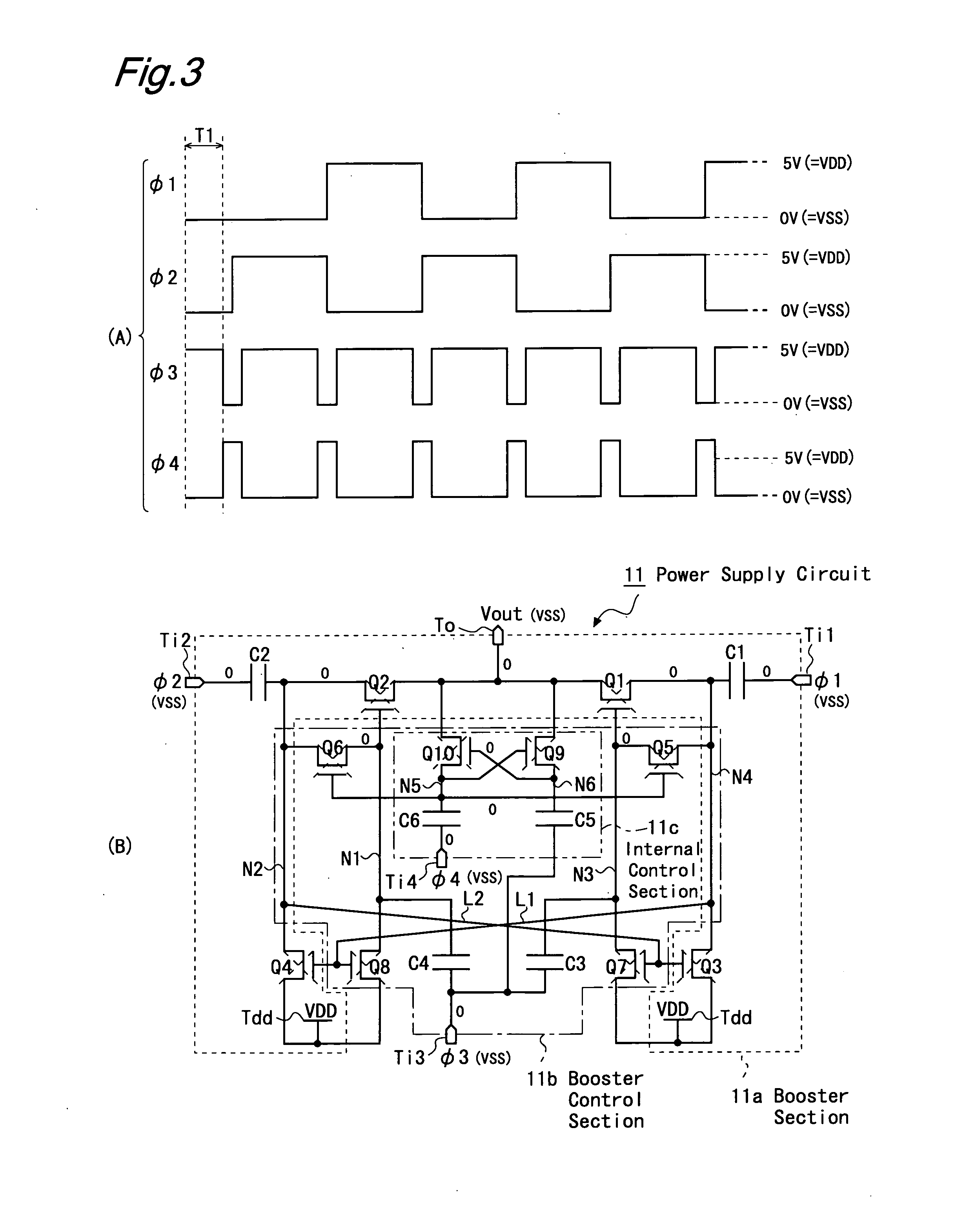
clock signals each having the same amplitude as the other and a voltage alternating oppositely to each other are supplied as the first and the second
clock signals to the first and the second input terminals respectively. Along with this, the third input terminal is supplied with the third
clock signal which has a voltage alternating between predetermined low and high levels with an amplitude greater than the
threshold voltage of the output-side switching element, and is maintained at the high level during its period except for a predetermined time near a time point at which there is a voltage change in the first and the second clock signals. In this arrangement, charging and boosting take place in the first capacitor and the second capacitor alternately and complementary to each other. Specifically, in one operation state a boosted voltage obtained at the first terminal of the first capacitor is outputted via the first switching element; in another operation state a boosted voltage obtained at the first terminal of the second capacitor is outputted via the second switching element; and these two operation states are repeated alternately to each other. While one of the first and the second capacitors is employed in boosting operation, the other is being charged. Such a complementary boosting cycle makes it possible to improve
electric current supply capability to a load.
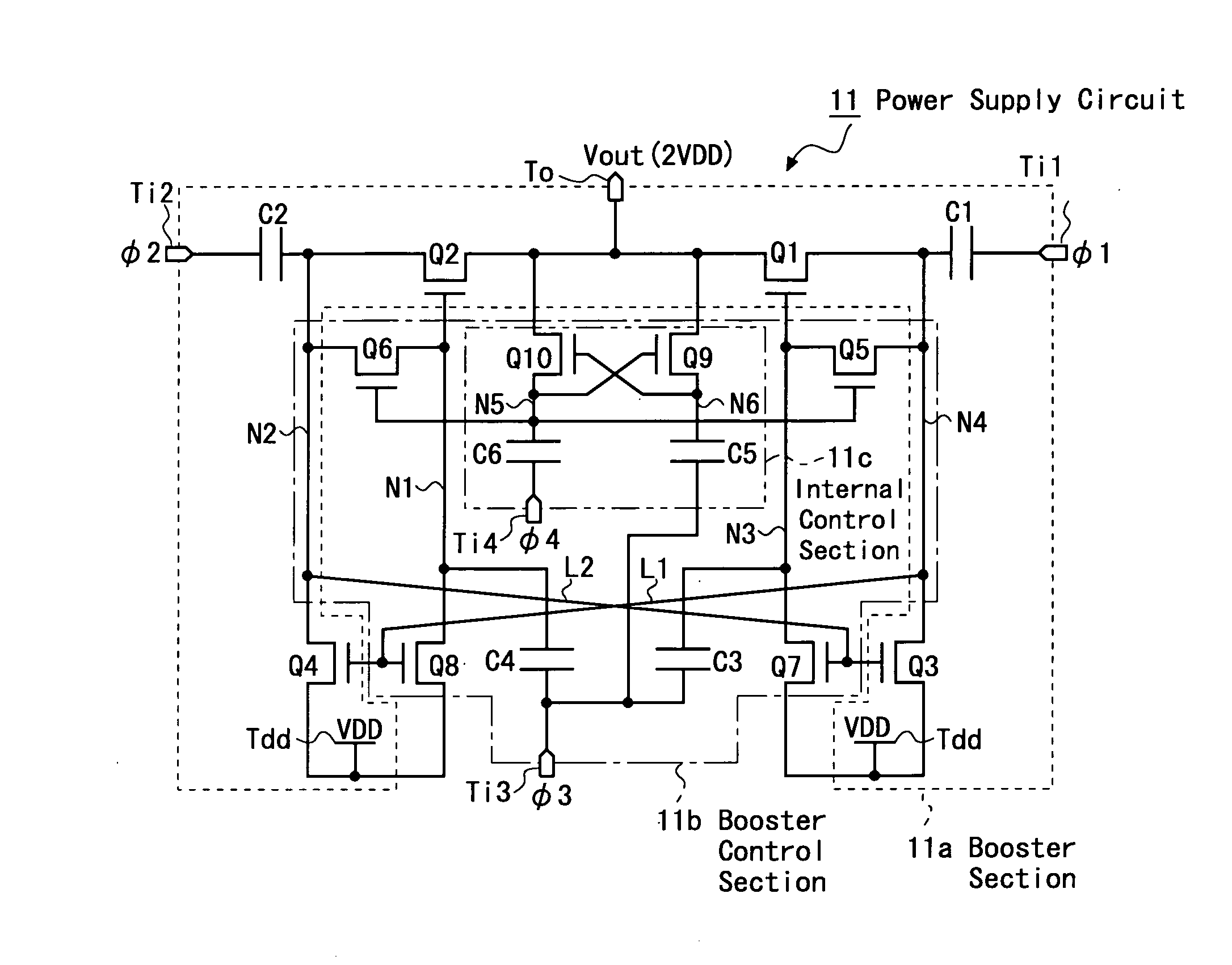
[0073]Also according to the third aspect of the present invention, when turning ON the first switching element which serves as the output-side switching element, a boosted voltage obtained at the first terminal of the first capacitor is supplied to the third capacitor and is boosted further by the third
clock signal, whereby a voltage which is higher than the originally boosted voltage by at least the threshold voltage of the first switching element is supplied to the control terminal of the first switching element. Likewise, when turning ON the second switching element which serves as the output-side switching element, a boosted voltage obtained at the first terminal of the second capacitor is supplied to the fourth capacitor and is boosted further by the third
clock signal, whereby a voltage which is higher than the originally boosted voltage by at least the threshold voltage of the second switching element is supplied to the control terminal of the second switching element. The arrangement ensures that the boosted voltages obtained at the respective first terminals of the first and the second capacitors are outputted as the boosted supply voltage without voltage drop by threshold value in the first and the second switching elements. Therefore, it is possible to output a desired boosted supply voltage reliably without being affected by the threshold voltage of the N-channel transistors or variation thereof even in cases where all of the switching elements in both of the booster section and the booster control section are provided by N-channel transistors.
[0074]According to the fourth aspect of the present invention, the third capacitor, which has its first terminal connected with the control terminal of the first switching element serving as the output-side switching element, is connected at its first terminal with the power supply terminal via the seventh switching element. This arrangement ensures that even in a case where the fifth switching element happens to have an unexpectedly large variation in its threshold value so as to be unable to turn ON the first switching element, it is still possible to turn ON the first switching element by boosting a voltage which is supplied to the third capacitor via the seventh switching element. Likewise, the fourth capacitor, which has its first terminal connected with the control terminal of the second switching element serving as the output-side switching element, is connected at its first terminal with the power supply terminal via the eighth switching element. This arrangement ensures that even in a case where the sixth switching element happens to have an unexpectedly large variation in its threshold value so as to be unable to turn ON the second switching element, it is still possible to turn ON the second switching element by boosting a voltage which is supplied to the fourth capacitor via the eighth switching element.
[0075]According to the fifth aspect of the present invention, when generating the voltage which is to be supplied to the control terminal of the output-side switching elements (the first and the second switching elements) in order to turn ON these switching elements, the boosted voltage is supplied from the main boosting capacitors (the first and the second capacitors) to the control-boosting capacitors (the third and the fourth capacitors) via the control-boosting switching elements (the fifth and the sixth switching elements). Meanwhile, the control terminal of the respective control-boosting switching elements (the fifth and the sixth switching elements) are supplied with a voltage which is higher than the said boosted voltage by at least the threshold voltage of the control-boosting switching elements. The arrangement makes it possible to reliably generate a voltage which is higher than the boosted voltage by at least the threshold voltage of the output-side switching element as a voltage that is to be supplied to the control terminal of the output-side switching element when turning ON the output-side switching element.
[0076]According to the sixth aspect of the present invention, a
clock signal of a voltage which changes oppositely to the third clock
signal and of an amplitude which is greater at least than a threshold voltage of the fifth and the sixth switching elements serving as the control-boosting switching element is supplied as the fourth clock
signal to the fourth input terminal, whereby the control-boosting switching elements have their respective control terminals supplied with a voltage which is higher than the boosted voltage obtained at the first terminal of the main boosting capacitor by at least the threshold voltage of the control-boosting switching element. Specifically, during a steady operation, the boosted supply voltage is held in the first and the second internal control capacitors, and when generating the voltage which is to be supplied to the control terminals of the output-side switching elements in order to turn ON these switching elements, the boosted voltage is supplied from the main boosting capacitors to the control-boosting capacitors via the control-boosting switching elements. In this process, the boosted supply voltage which is obtained at the first terminal of the second internal control capacitor is boosted by the fourth clock signal. Thus, the control terminal of the control-boosting switching element is supplied with a voltage which is higher than the originally boosted voltage by at least the threshold voltage of the control-boosting switching elements. This eliminates voltage drop by threshold value in the control-boosting switching elements, ensuring reliable generation of a voltage which is higher than the boosted voltage by at least the threshold voltage of the output-side switching element as a voltage that is to be supplied to the control terminal of the output-side switching element when turning ON the output-side switching element.
[0077]According to the seventh aspect of the present invention, since there is no voltage drop by threshold value in the output-side switching element of the boosting section even if the switching elements are solely provided by N-channel transistors, it is possible to form a power supply circuit which is capable of outputting a desired boosted supply voltage reliably, on an insulated substrate such as a glass substrate, using N-channel transistors made of polycrystal
silicon whose threshold value is higher and variation thereof is wider than those made of monocrystal
silicon.
[0078]According to the eighth aspect of the present invention, since there is no voltage drop by threshold value in the output-side switching element of the boosting section even if the switching elements are solely provided by N-channel transistors, it is possible to form a power supply circuit which is capable of outputting a desired boosted supply voltage reliably, on an insulated substrate such as a glass substrate, using N-channel transistors provided by thin film transistors whose threshold value is higher and variation thereof is wider than those made of monocrystal
silicon.
[0079]According to the ninth aspect of the present invention, a driver monolithic
display device includes a substrate formed thereon with a
voltage boosting power supply circuit together with a plurality of pixel circuits and at least part of a
driving circuit. In this configuration, the power supply circuit uses N-channel transistors for all of its switching elements, and yet is capable of outputting a desired boosted supply voltage reliably without a voltage drop by threshold value. Thus, the present invention enables
size reduction of display devices and cost reduction in the manufacture thereof.
[0080]According to the tenth aspect of the present invention, a driver monolithic
display device includes a substrate formed thereon with a
voltage boosting power supply circuit together with a plurality of pixel circuits and at least part of a
driving circuit. In this configuration, the power supply circuit is capable of outputting a desired boosted supply voltage reliably without a voltage drop by threshold value. Further, switching elements constituting these pixel circuits, the part of
driving circuit and the power supply circuit which are formed on the same substrate are solely provided by N-channel thin film transistors. This enables simultaneous formation and cost reduction thereby of these circuits, to be achieved through a fewer number of manufacturing steps than necessary for cases which require both N-channel thin film transistors and P-channel thin film transistors.

