[0003]It is therefore an object of the present invention to provide an organic light-emitting device where the injection of charge carriers can be adjusted independently from the operation
voltage.
[0013]With independently adjustable
charge injection (via UEB) and charge transport (via UCB), position and width of the recombination zone can be varied while maintaining a good
charge carrier balance partly predetermined by the present layer stack and layer materials. Variations in
layer thickness, material composition, material properties of the
organic layer stack leading to the previously described problems can now be easily compensated by suitable adjustment of UEB and UCB. A well-placed recombination zone and a simultaneously well maintained / adjusted charge carrier balance maximize the efficiency w.r.t. light output and minimize negative effects on life-time due to charge carriers penetrating the recombination zone towards the opposite electrode. Eventually,
electron and / or hole blocking layers can be avoided because of a well-adjusted charge carrier balance, which reduces the preparation effort and therefore preparation costs. The load of the hole transporting layer with electrons or
electron transporting layers with holes can be reduced or ideally avoided. Another
advantage is the low required
voltage UEB to control the current flow through the
organic layer stack. The
OLED device according to the present invention is switchable fast between a “light-on” and a “light-off” mode, and the switched base current can be significantly smaller than the total
OLED (C and E) current. In the “light-on” mode the second electrode injects charge carriers into the organic layer, while in the “light-off” mode the first electrode injects no charge carriers or a negligible amount of charge carriers into the organic layer. The properties of
charge carrier injection of the second electrode will not be influenced by switching the first electrode between light-on mode and light-off mode.
[0017]In another embodiment, the organic light-emitting layer comprises at least a first sub-layer suitable to emit light of a first color and a second sub-layer to emit light of a second color different to the first color. Here, a shift of the recombination zone by suitable adjusting of UEB and UCB enables an adjustment of the color point of the emitted light. For a first set of UEB and UCB, the recombination zone may be located mainly within the first sub-layer leading to a
light emission dominated by the first color. For a second set of UEB and UCB, the recombination zone may be located mainly within the second sub-layer leading to a
light emission dominated by the second color. The same modification is applicable for three or more different sub-layers emitting light of three or more colors to adjust / modify the color point of the superposed light emitted from the
OLED device. To achieve light emission of a certain color, it is also possible to operate the OLED in a switched mode, i.e. modulating the emission color under control of UEB and UCB with a
switching frequency high enough to ensure a constant color impression by the
human eye.
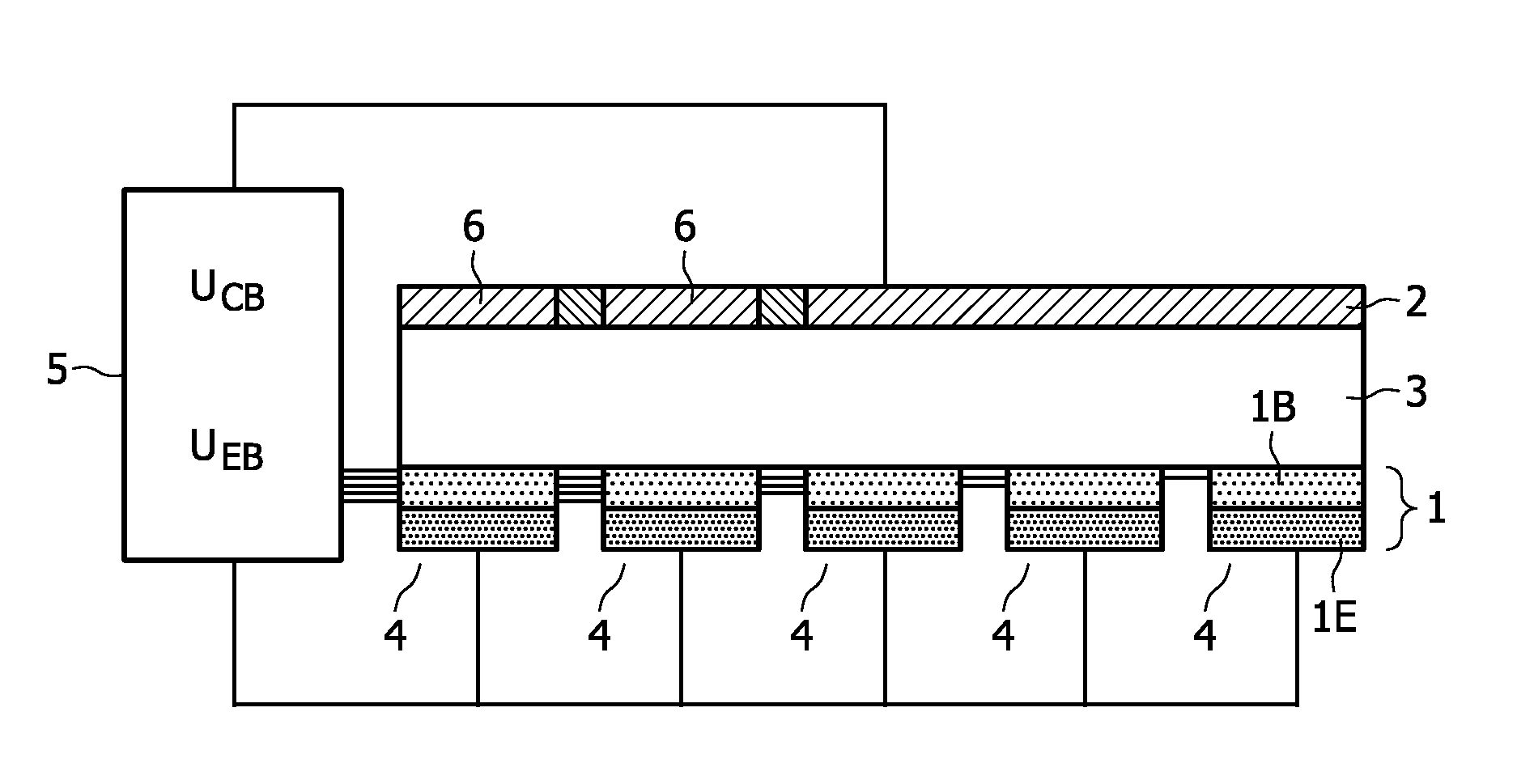
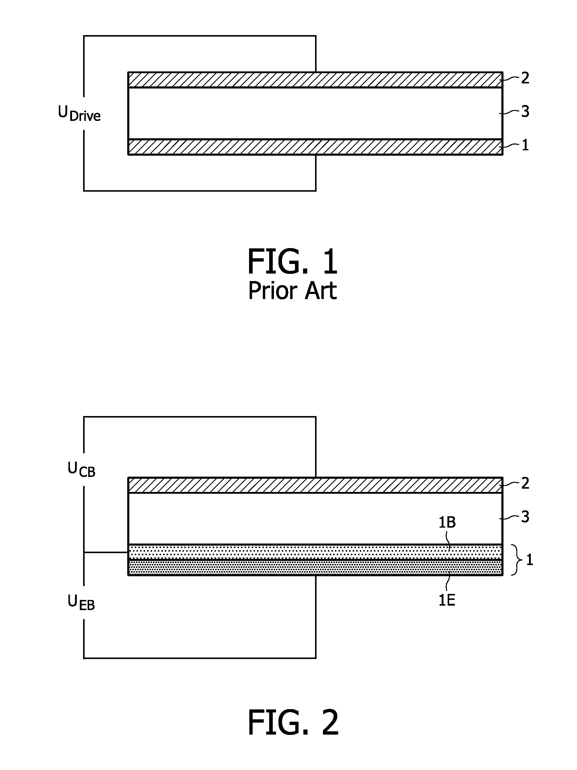
[0023]First and second voltages UCB and UEB are adjusted independently. Charge carriers are electrons and holes. A suitable separate adjustment of first and second voltage strongly reduces the probability for charge carriers to reach the opposite electrode leading to a more efficient OLED operation. Charge carriers reaching the opposite electrodes are lost for light generation within the organic light-emitting layer. The organic layer stack located between first and second electrode may comprise only one light-emitting layer. In other embodiments, the organic layer stack may comprise additional layers such as hole / electron transport layers, hole /
electron injection layers and / or hole / electron blocking layers as well as different organic light-emitting layers emitting light of different colors. Furthermore, the method enables to operate the OLED in a way, where layers mainly designed for transport of one type of charge carriers are at least less loaded with the other type of charge carriers resulting in a better lifetime performance of these layers. The method above may enable to reduce the number of organic layers of an OLED device by avoiding charge carrier blocking layers.
[0024]In an embodiment, the method comprises the step of selecting a suitable first and second voltage to adjusting the position and / or width of a recombination zone to be essentially located within the organic light-emitting layer. In this embodiment, a further improvement of the OLED lifetime will be achieved together with an improved efficiency of the light generation within the organic light-emitting layer. The recombination energy will be released at that location, where the emitting molecules are present. Within the recombination zone, the majority of electrons and holes are bound and therefore cannot penetrate to layers, where the presence of these charge carriers is not desired. The term “essentially” relates to the ratio between thickness of the organic light-emitting layer and the width of the recombination zone. Here, “essentially” corresponds to a ratio of more than 0.8, preferably more than 0.9, more preferred more than 1.0.
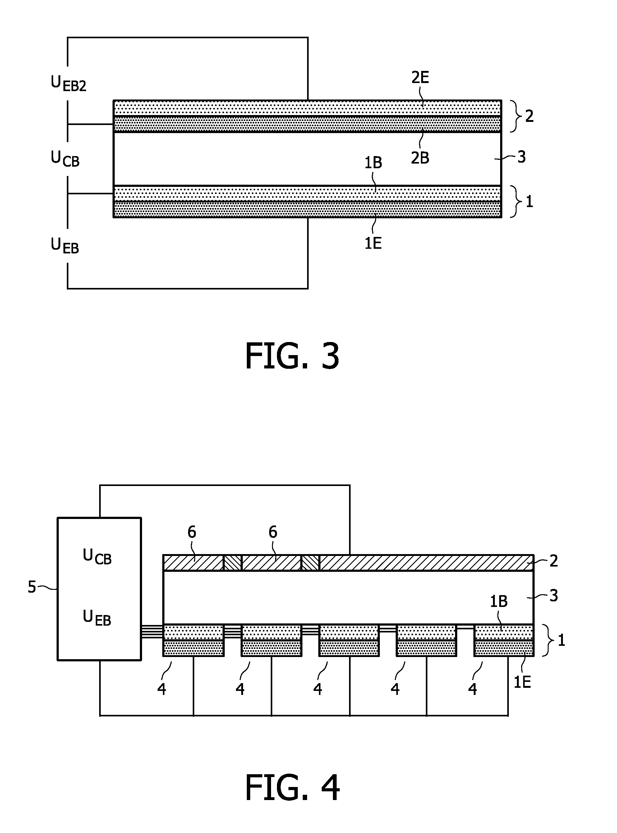
[0028]If the injection properties of both charge carriers, electrons and holes, can be controlled via UEB and UEB2, the adjustment of width and position of the recombination zone can be performed more precisely.

