Method for forming tungsten contacts and interconnects with small critical dimensions

Inactive Publication Date: 2010-10-21
NOVELLUS SYSTEMS
View PDF100 Cites 80 Cited by
  • Summary
  • Abstract
  • Description
  • Claims
  • Application Information

AI Technical Summary

Benefits of technology

[0004]One aspect of the invention relates to methods of void-free tungsten fill of high aspect ratio features. According to various embodiments, the methods involve a reduced temperature chemical vapor deposition (CVD) process to fill the features with tungsten. In certain embodiments, the process temperature is maintained at less than about 350° C. during the chemical vapor deposition to fill the feature. The reduced-temperature CVD tungsten fill provides improved tungsten fill in high aspect ratio features, provides improved

Problems solved by technology

As semiconductor devices scale to the 32 nm technology node and beyond, shrinking contact and via dimensions make chemical vapor deposition of tungsten more challenging.
Increasing aspect ratios can lead to voids or large seams w

Method used


Image

  • Method for forming tungsten contacts and interconnects with small critical dimensions
  • Method for forming tungsten contacts and interconnects with small critical dimensions
  • Method for forming tungsten contacts and interconnects with small critical dimensions

Examples


Embodiment Construction

Introduction

[0025]In the following description, numerous specific details are set forth in order to provide a thorough understanding of the present invention, which pertains to forming thin tungsten films. Modifications, adaptations or variations of specific methods and structures shown and discussed herein will be apparent to those skilled in the art and are within the scope of this invention.

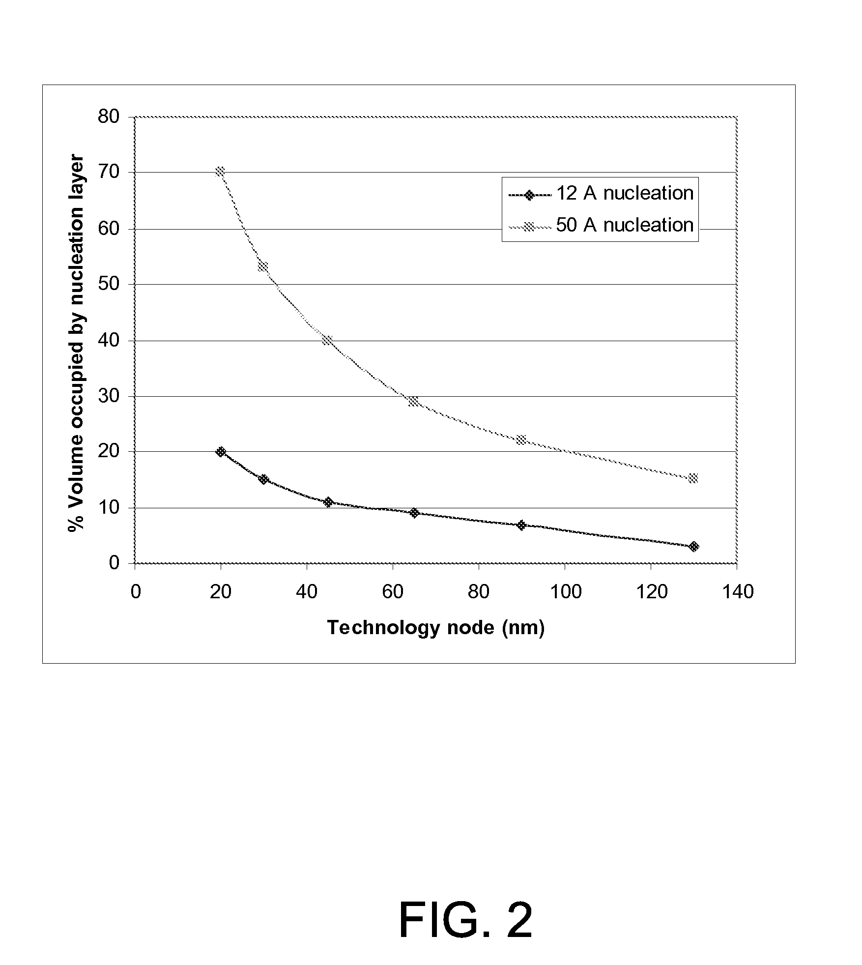
[0026]Extending tungsten to sub-32 nm technologies is critical to maintaining via / contact performance and reliability in both memory and logic devices. There are various challenges in tungsten fill as devices scale to smaller technology nodes. One challenge is preventing an increase in resistance due to the thinner films in contacts and vias. As features become smaller, the tungsten (W) contact or line resistance increases due to scattering effects in the thinner W film. While efficient tungsten deposition processes require tungsten nucleation layers, these layers typically have higher electri...


PUM

PropertyMeasurementUnit
Temperatureaaaaaaaaaa

Abstract

Provided are methods of void-free tungsten fill of high aspect ratio features. According to various embodiments, the methods involve a reduced temperature chemical vapor deposition (CVD) process to fill the features with tungsten. In certain embodiments, the process temperature is maintained at less than about 350° C. during the chemical vapor deposition to fill the feature. The reduced-temperature CVD tungsten fill provides improved tungsten fill in high aspect ratio features, provides improved barriers to fluorine migration into underlying layers, while achieving similar thin film resistivity as standard CVD fill. Also provided are methods of depositing thin tungsten films having low-resistivity. According to various embodiments, the methods involve performing a reduced temperature low resistivity treatment on a deposited nucleation layer prior to depositing a tungsten bulk layer and/or depositing a bulk layer via a reduced temperature CVD process followed by a high temperature CVD process.

Description

CROSS-REFERENCE TO RELATED APPLICATION[0001]This application claims the benefit under U.S.C. 119(e) to U.S. provisional application 61 / 169,954 filed Apr. 16, 2009, titled “METHOD FOR FORMING TUNGSTEN CONTACTS AND INTERCONNECTS WITH SMALL CRITICAL DIMENSIONS,” the entirety of which is incorporated herein by this reference.BACKGROUND[0002]The deposition of tungsten films using chemical vapor deposition (CVD) techniques is an integral part of many semiconductor fabrication processes. Tungsten films may be used as low resistivity electrical connections in the form of horizontal interconnects, vias between adjacent metal layers, and contacts between a first metal layer and the devices on the silicon substrate. In a conventional tungsten deposition process, the wafer is heated to the process temperature in a vacuum chamber, and then a very thin portion of tungsten film, which serves as a seed or nucleation layer, is deposited. Thereafter, the remainder of the tungsten film (the bulk layer...

Claims


Application Information

Patent Timeline
IPC IPC(8): H01L21/768B05C11/00
CPCC23C16/0272C23C16/045C23C16/14C23C16/45523H01L21/76879H01L21/76876H01L21/76877H01L21/67017H01L21/76843H01L21/28556H01L2924/0002H01L2924/00C23C16/52H01L21/76816H01L21/76895H01L23/53266H01L23/535
Inventor CHANDRASHEKAR, ANANDCHEN, FENGHUMAYUN, RAASHINADANEK, MICHAL
Owner NOVELLUS SYSTEMS
Why Eureka
Try Eureka